Piezoelectric bulk wave device, and method of manufacturing the piezoelectric bulk wave device

a technology of bulk wave and piezoelectric, which is applied in the direction of piezoelectric/electrostrictive transducers, generators/motors, transducer types, etc., can solve the problems of large variations in electrical characteristics and difficulty in obtaining good electrical characteristics, and achieve small fluctuations in electromechanical coupling coefficients, small variations in characteristics, and small variations in characteristics

Active Publication Date: 2014-06-26
MURATA MFG CO LTD
View PDF6 Cites 6 Cited by
  • Summary
  • Abstract
  • Description
  • Claims
  • Application Information

AI Technical Summary

Benefits of technology

[0006]It is an object of the present invention to provide a piezoelectric bulk wave device that utilizes the thickness shear mode of LiTaO3, and exhibits relatively small variations in electrical characteristics caused by variations in electrode film thickness or in the thickness of LiTaO3, and a method of manufacturing the piezoelectric bulk wave device.
[0011]In this case, the position of the high concentration ion-implanted portion can be easily controlled by selecting the above-mentioned ion implantation conditions. Generally, an ion beam from an ion implantation device is linearly applied to the substrate with uniform intensity, and the ion beam is applied a number of times at substantially the same irradiation angle to the same location while scanning the entire substrate. Accordingly, in comparison to thickness variations due to film deposition methods such as sputtering, CVD, and evaporation, by using ion implantation, the position of the high concentration ion-implanted portion becomes uniform over the entire substrate surface, leading to smaller variations in depth. Therefore, it is possible to easily obtain a piezoelectric thin plate with an accurate thickness over the entire substrate surface.
[0013]In this case, it is possible to reduce the possibility of a defect occurring in the piezoelectric thin plate due to thermal stress exerted when separating the piezoelectric thin plate.
[0015]According to the present invention, the first and second electrodes are each formed by a conductor having a specific acoustic impedance higher than the specific acoustic impedance of a transversal wave that propagates in LiTaO3, and when the sum of the film thicknesses of the first and second electrodes is defined as an electrode thickness, and the thickness of the piezoelectric thin plate made of LiTaO3 is defined as an LT thickness, the electrode thickness / (electrode thickness+LT thickness) is in the range of not less than 5% and not more than 40%. Therefore, it is possible to provide a piezoelectric bulk wave device that exhibits relatively small fluctuations in electromechanical coupling coefficient. Accordingly, it is possible to provide a piezoelectric bulk wave device with relatively small variations in characteristics.
[0016]In the method of manufacturing a piezoelectric bulk wave device according to the present invention, the first and second electrodes are configured in the manner as mentioned above. Therefore, in accordance with the present invention, it is possible to provide a piezoelectric bulk wave device with relatively small variations in characteristics.

Problems solved by technology

However, in a case where the thickness shear mode is utilized by using a piezoelectric thin film made of LiTaO3, it is difficult to obtain good electrical characteristics.
Moreover, manufacturing variations in LiTaO3 or electrode film thickness tend to lead to large variations in electrical characteristics.

Method used


Image

  • Piezoelectric bulk wave device, and method of manufacturing the piezoelectric bulk wave device
  • Piezoelectric bulk wave device, and method of manufacturing the piezoelectric bulk wave device
  • Piezoelectric bulk wave device, and method of manufacturing the piezoelectric bulk wave device

Examples


Embodiment Construction

[0041]Hereinafter, the present invention will be explained by way of specific embodiments of the present invention with reference to the drawings.

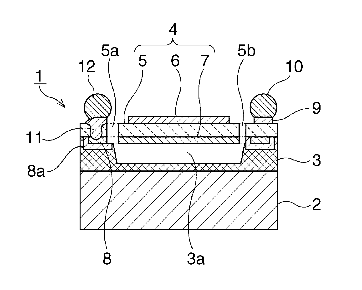
[0042]FIGS. 1(a) and 1(b) are a schematic elevational cross-sectional view and a plan view, respectively, of a piezoelectric bulk wave device according to an embodiment of the present invention.

[0043]A piezoelectric bulk wave device 1 according to this embodiment has a support substrate 2. The support substrate 2 is formed by a suitable insulating body or piezoelectric body. In this embodiment, the support substrate 2 is formed by alumina.

[0044]An insulating layer 3 is formed on the support substrate 2. While the insulating layer 3 is made of silicon oxide in this embodiment, the insulating layer 3 may be made of a suitable insulating material such as LiTaO3, LiNbO3, sapphire, or glass. Alumina, glass, and LiNbO3 are preferred because these materials are inexpensive in comparison to LiTaO3 and sapphire, and easy to manufacture. A recess 3a...


PUM

PropertyMeasurementUnit
Euler Anglesaaaaaaaaaa
resonant frequencyaaaaaaaaaa

Abstract

A piezoelectric bulk wave device that includes a piezoelectric thin plate that is made of LiTaO3, and first and second electrodes that are provided in contact with the piezoelectric thin plate. The piezoelectric bulk wave device utilizes the thickness shear mode of the piezoelectric thin plate made of LiTaO3. The first and second electrodes are each formed by a conductor having a specific acoustic impedance higher than the specific acoustic impedance of a transversal wave that propagates in LiTaO3. When the sum of the film thicknesses of the first and second electrodes is defined as an electrode thickness, and the thickness of the piezoelectric thin plate made of LiTaO3 is defined as an LT thickness, the electrode thickness / (electrode thickness+LT thickness) is not less than 5% and not more than 40%.

Description

CROSS REFERENCE TO RELATED APPLICATIONS[0001]The present application is a continuation of International application No. PCT / JP2012 / 071576, filed Aug. 27, 2012, which claims priority to Japanese Patent Application No. 2011-190342, filed Sep. 1, 2011, the entire contents of each of which are incorporated herein by reference.FIELD OF THE INVENTION[0002]The present invention relates to a piezoelectric bulk wave device using LiTaO3, and a method of manufacturing the piezoelectric bulk wave device. More specifically, the present invention relates to a piezoelectric bulk wave device that utilizes a bulk wave of thickness shear mode as a bulk wave, and a method of manufacturing the piezoelectric bulk wave device.BACKGROUND OF THE INVENTION[0003]In related art, piezoelectric thin film devices are used for oscillators, filters, and the like. For example, a piezoelectric thin film device illustrated in FIG. 24 is disclosed in Patent Document 1 mentioned below. A piezoelectric thin film device ...

Claims


Application Information

Patent Timeline
Patent Type & Authority Applications(United States)
IPC IPC(8): H01L41/187H01L41/29H01L41/047
CPCH03H3/02H03H9/02157H03H9/0595H03H9/173Y10T29/42H10N30/8536H10N30/06H10N30/877
Inventor KANDO, HAJIME
Owner MURATA MFG CO LTD
Why Eureka
Try Eureka