Multi-Level Memory Array Having Resistive Elements For Multi-Bit Data Storage

a multi-level memory array and resistive element technology, applied in digital storage, electrical equipment, instruments, etc., can solve the problems of only allowing limited programming on the diode, scaling issues pose challenges for traditional nonvolatile memory technology,

Inactive Publication Date: 2014-06-26
SANDISK TECH LLC +2
View PDF5 Cites 31 Cited by
  • Summary
  • Abstract
  • Description
  • Claims
  • Application Information

AI Technical Summary

Benefits of technology

[0012]In one embodiment, the resistor array includes two or more resistive elements and two or more electrode layers. In other embodiment, the resistor array further includes a multiplexer connected to each of the two or more resistive elements. Each resistive element can be electrically turned on to be at an “on” resistance state with its resistance value, such that the two or more resistive elements can be selectively connected in 2N numbers of different combinations and provide 2N number of possible resistance values as a total resistance of the resistor array provided to control the resistance of any of the one or more resistive switching memory elements of the memory device. Accordingly, the resistor array is capable of controlling the total resistance of the memory device and placing a resistive switching memory element connected thereto at 2N number of different resistance states.

Problems solved by technology

However, as device dimensions shrink, scaling issues pose challenges for traditional nonvolatile memory technology.
The diode only allows limited programming and erasing currents to pass through the resistive switching memory element in desired directions.

Method used


Image

  • Multi-Level Memory Array Having Resistive Elements For Multi-Bit Data Storage
  • Multi-Level Memory Array Having Resistive Elements For Multi-Bit Data Storage
  • Multi-Level Memory Array Having Resistive Elements For Multi-Bit Data Storage

Examples


Embodiment Construction

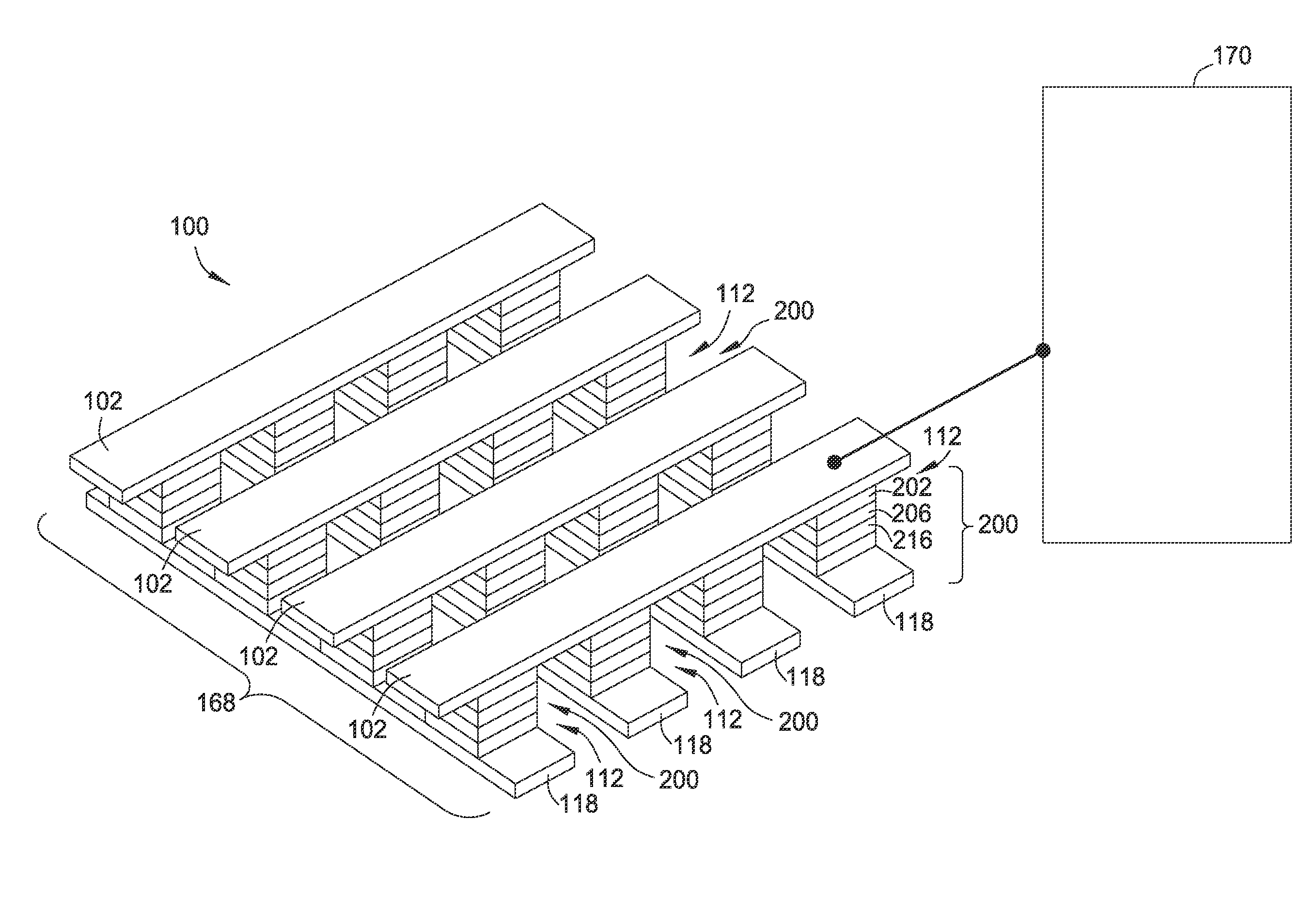
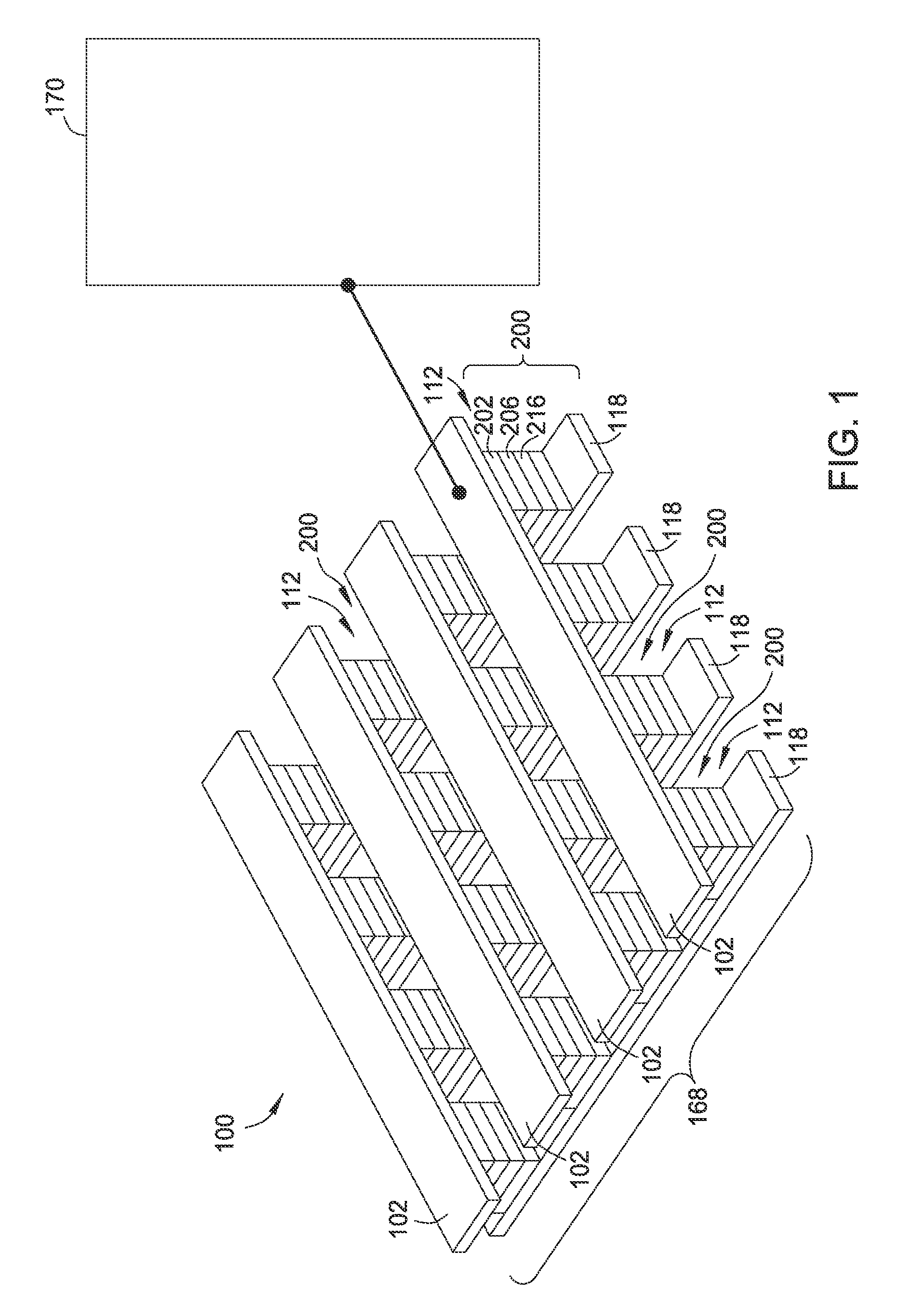
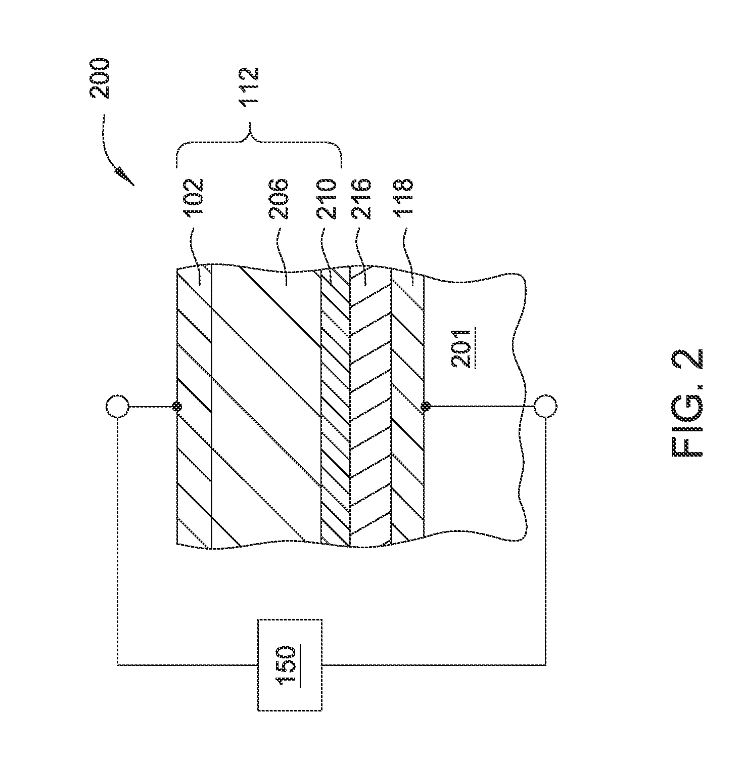
[0027]Certain embodiments include a method of using a resistor array in an array of resistive switching memory cells and memory devices to store more than 1 bit of data information in a selectively controllable manner. The resistor array is electrically connected to at least one resistive switching memory device, resistive switching memory cell, or resistive switching memory element. In one embodiment, each memory array or memory device includes one or more resistive switching memory cells or one or more resistive switching memory elements. Each resistive switching memory cell may include a resistive switching memory element.

[0028]In one aspect of the invention, the resistance state of a memory device, a resistive switching memory cell, or a resistive switching memory element is controlled by the total resistance of the resistor array such that each memory device, resistive switching memory cell, or resistive switching memory element can be selectively is configured to store N bits ...


PUM


Abstract

A resistor array for multi-bit data storage without the need to increase the size of a memory chip or scale down the feature size of a memory cell contained within the memory chip is provided. The resistor array incorporates a number of discrete resistive elements to be selectively connected, in different series combinations, to at least one memory cell or memory device. In one configuration, by connecting each memory cell or device with at least one resistor array, a resistive switching layer found in the resistive switching memory element of the connected memory device is capable of being at multiple resistance states for storing multiple bits of digital information. During device programming operations, when a desired series combination of the resistive elements within the resistor array is selected, the resistive switching layer in the connected memory device can be in a desired resistance state.

Description

BACKGROUND[0001]1. Technical Field[0002]Provided are methods of forming resistive switching memory devices and arrays and storing N bits of data in resistive switching memory devices. Provided also are various structural features of resistive switching memory devices and arrays.[0003]2. Description of the Related Art[0004]Nonvolatile memory devices are used in systems in which persistent storage is required. For example, nonvolatile memory cards are used in digital cameras to store images and in digital music players to store audio data. Nonvolatile memory devices are also used to persistently store data in computer environments.[0005]Electrically-erasable programmable read only memory (EEPROM) technology is often used to form and program nonvolatile memory devices. This type of nonvolatile memory contains floating gate transistors that can be selectively programmed or erased by application of suitable voltages to their terminals. As fabrication techniques improve, it is becoming po...

Claims


Application Information

Patent Timeline
Patent Type & Authority Applications(United States)
IPC IPC(8): G11C13/00H01L45/00
CPCG11C11/5685G11C2213/32G11C2213/33G11C2213/34G11C2213/72G11C13/0069H10B63/84H10B63/20H10B63/30H10N70/883H10N70/021G11C7/1051G11C13/0007G11C7/1006G11C7/1078G11C7/22G11C7/12G11C11/56G11C13/004
Inventor PRAMANIK, DIPANKARLAZOVSKY, DAVID E.MINVIELLE, TIMYAMAGUCHI, TAKESHI
Owner SANDISK TECH LLC
Why Eureka
Try Eureka