Silicon nitride gapfill implementing high density plasma

a technology of silicon nitride and high density plasma, which is applied in the direction of coating, chemical vapor deposition coating, metallic material coating process, etc., can solve the problems of dielectric material, dielectric material, and structural features of the device having decreased spatial dimensions,

Inactive Publication Date: 2014-07-03
APPLIED MATERIALS INC
View PDF9 Cites 248 Cited by
  • Summary
  • Abstract
  • Description
  • Claims
  • Application Information

AI Technical Summary

Problems solved by technology

The decreasing feature sizes result in structural features on the device having decreased spatial dimensions.
The widths of gaps and trenches on the device narrow to a point where the aspect ratio of gap depth to its width becomes high enough to make it challenging to fill the gap with dielectric material.
The depositing dielectric material is prone to clog at the top before the gap completely fills, producing a void or seam in the middle of the gap.
The high reactivity of the species in the plasma reduces the energy required to activate a chemical reaction.
Depositing silicon nitride by HDP-CVD has been found to produce highly compressive films which can distort or damage intricate features around silicon nitride filled trenches.

Method used


Image

  • Silicon nitride gapfill implementing high density plasma
  • Silicon nitride gapfill implementing high density plasma
  • Silicon nitride gapfill implementing high density plasma

Examples


Embodiment Construction

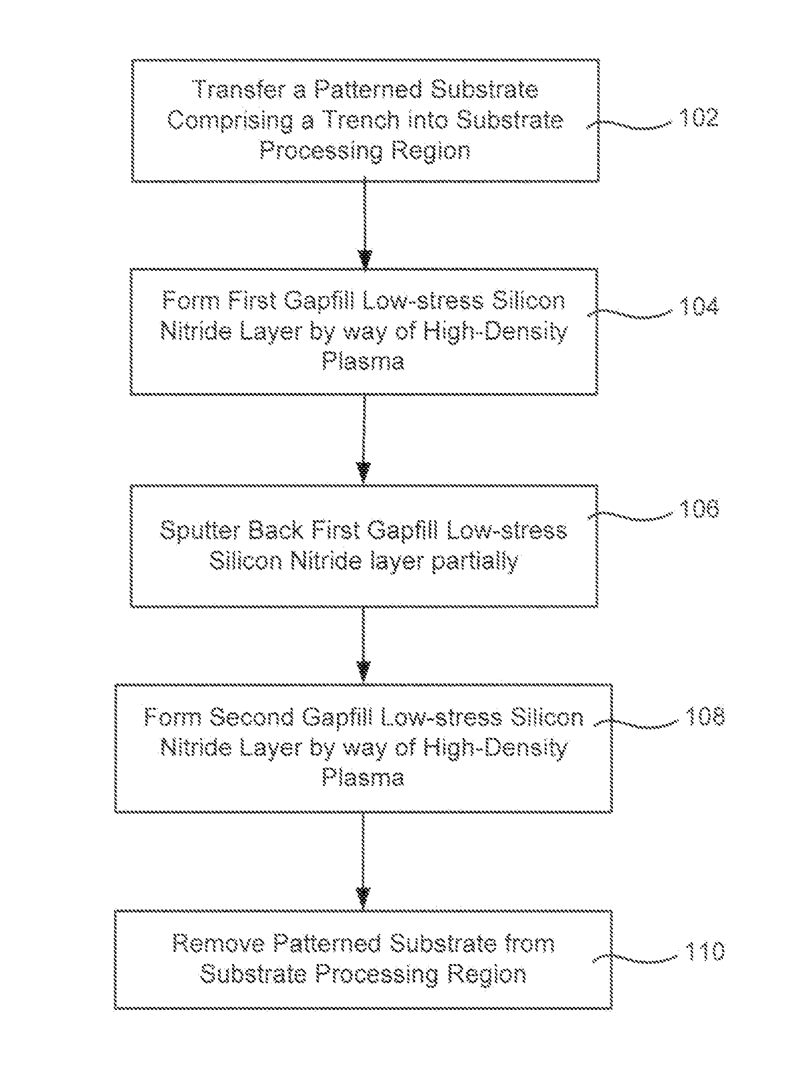
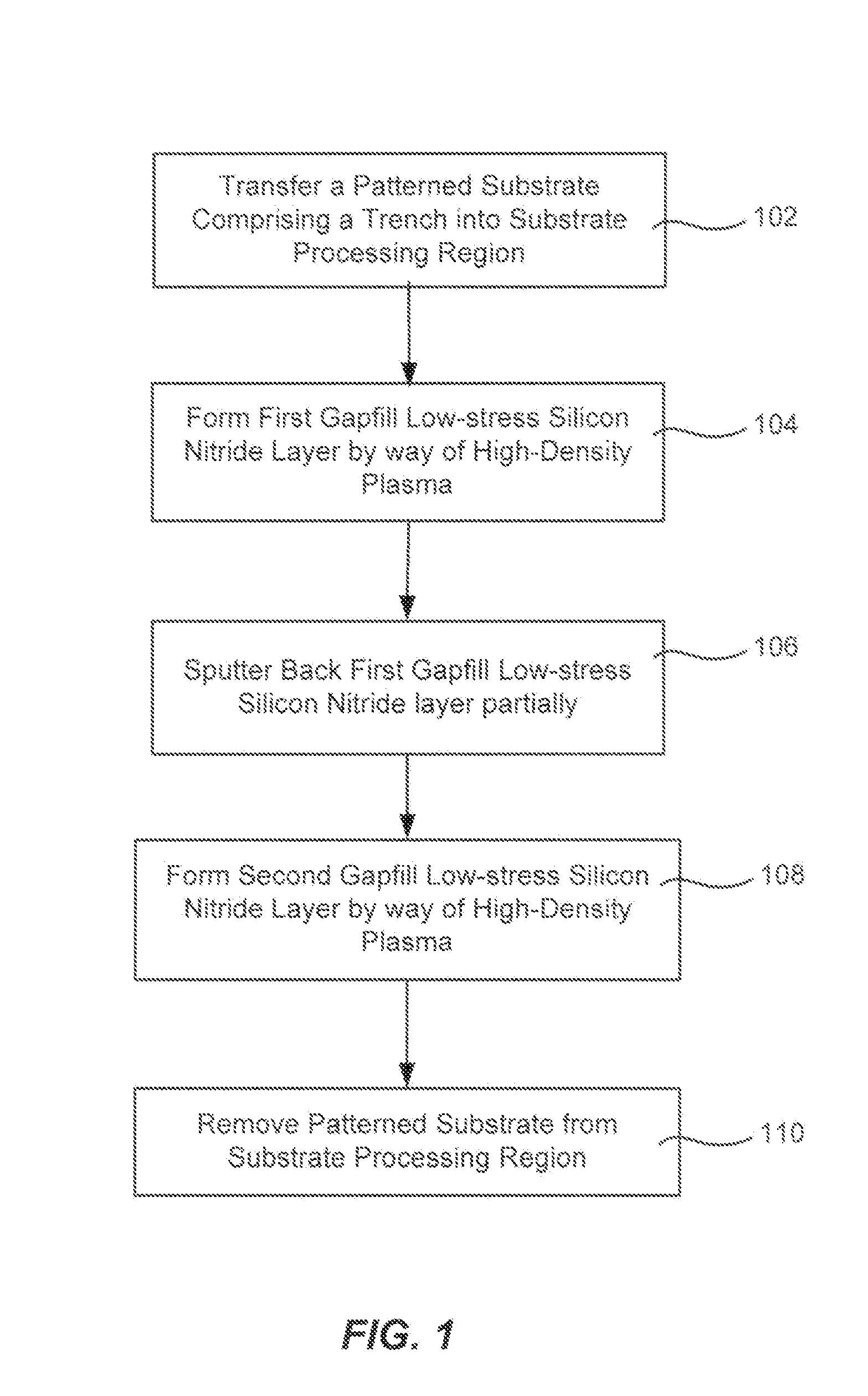
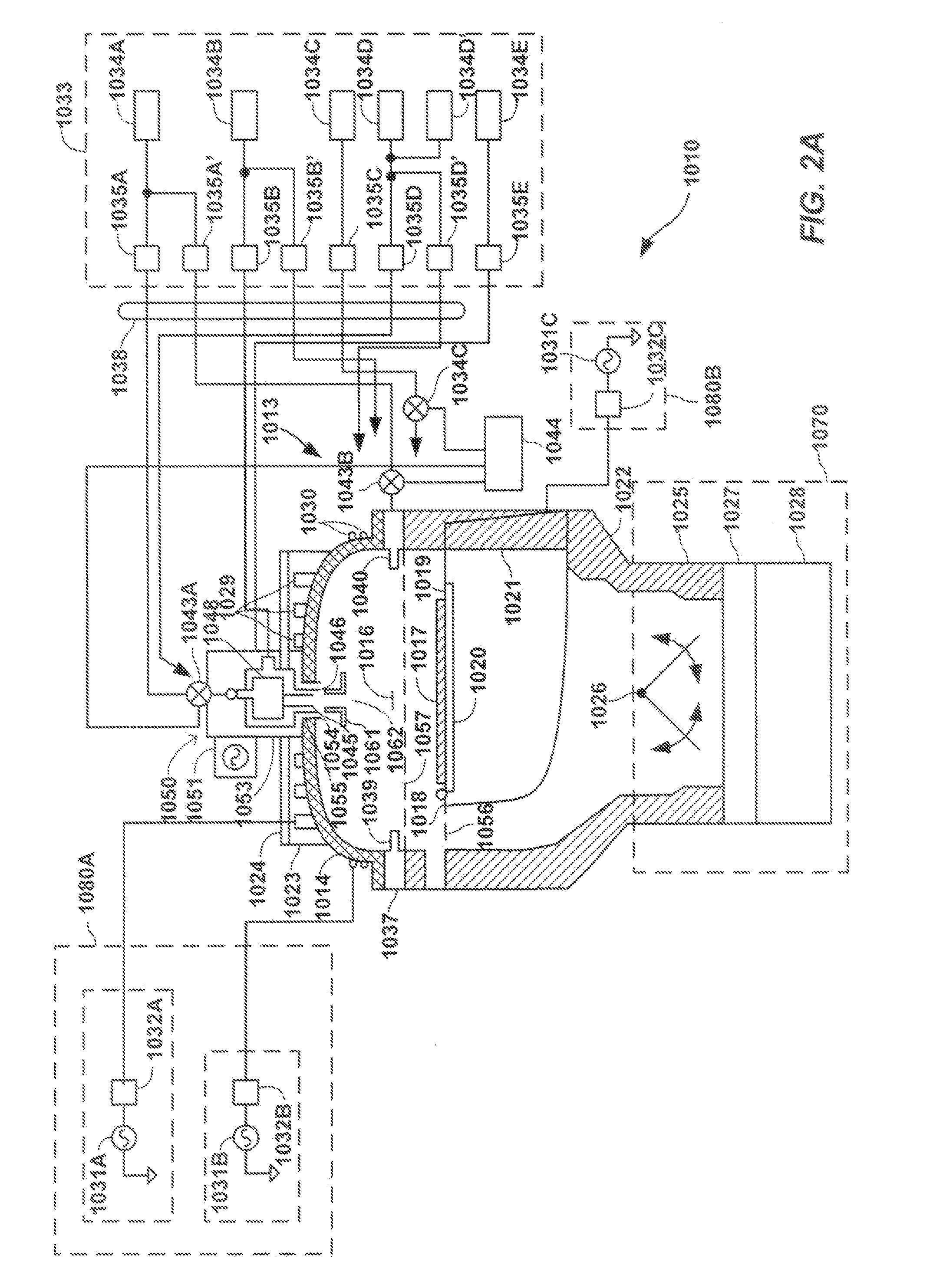
[0013]Methods of filling features with silicon nitride using high-density plasma chemical vapor deposition are described. Narrow trenches may be filled with gapfill silicon nitride without damaging compressive stress. A low but non-zero bias power is used during deposition of the gapfill silicon nitride. An etch step is included between each pair of silicon nitride high-density plasma deposition steps in order to supply sputtering which would normally be supplied by high bias power.

[0014]Methods of depositing silicon nitride on patterned substrates have been developed using high-density plasma techniques. Methods of filling trenches with gapfill silicon nitride layers have been developed for patterned substrates. Applying nonzero but relatively low bias power during deposition has been found to reduce stress yet still enable silicon nitride to fill gaps in high aspect ratio trenches. Interleaving a sputtering / etching step between otherwise adjacent low-bias SiN HDP steps has been fo...


PUM

PropertyMeasurementUnit
bias poweraaaaaaaaaa

Abstract

Methods of filling features with silicon nitride using high-density plasma chemical vapor deposition are described. Narrow trenches may be filled with gapfill silicon nitride without damaging compressive stress. A low but non-zero bias power is used during deposition of the gapfill silicon nitride. An etch step is included between each pair of silicon nitride high-density plasma deposition steps in order to supply sputtering which would normally be supplied by high bias power.

Description

[0001]This application claims the benefit of U.S. Prov Pat. App. No. 61 / 748,276 filed Jan. 2, 2013, and titled “METAL PROCESSING USING HIGH DENSITY PLASMA,” as well as U.S. Prov Pat. App. No. 61 / 751,629 filed Jan. 11, 2013, and titled “SILICON NITRIDE GAPFILL IMPLEMENTING HIGH DENSITY PLASMA.” Each of the above applications is hereby entirely incorporated herein by reference for all purposes.BACKGROUND OF THE INVENTION[0002]Semiconductor device geometries have dramatically decreased in size since their introduction several decades ago. Modern semiconductor fabrication equipment routinely produce devices with 32 nm, 28 nm and 22 nm feature sizes, and new equipment is being developed and implemented to make devices with even smaller geometries. The decreasing feature sizes result in structural features on the device having decreased spatial dimensions. The widths of gaps and trenches on the device narrow to a point where the aspect ratio of gap depth to its width becomes high enough t...

Claims


Application Information

Patent Timeline
Patent Type & Authority Applications(United States)
IPC IPC(8): H01L21/02
CPCH01L21/0217H01L21/02266H01L21/02274C23C16/045C23C16/345C23C16/507H01L21/02063H01L21/02301H01L21/02315
Inventor HUA, ZHONG QIANGLE, HIEN MINHLEE, YOUNG
Owner APPLIED MATERIALS INC
Why Eureka
Try Eureka