Global low power capture scheme for cores

a power capture scheme and core technology, applied in the field of integrated circuit testing, can solve the problems of significant yield loss, flip-flops and gates acting incorrectly, high cost of scan based testing, etc., and achieve the effect of reducing peak power, high defect coverage, and reducing peak power problems

Active Publication Date: 2014-07-03
NVIDIA CORP
View PDF7 Cites 4 Cited by
  • Summary
  • Abstract
  • Description
  • Claims
  • Application Information

AI Technical Summary

Benefits of technology

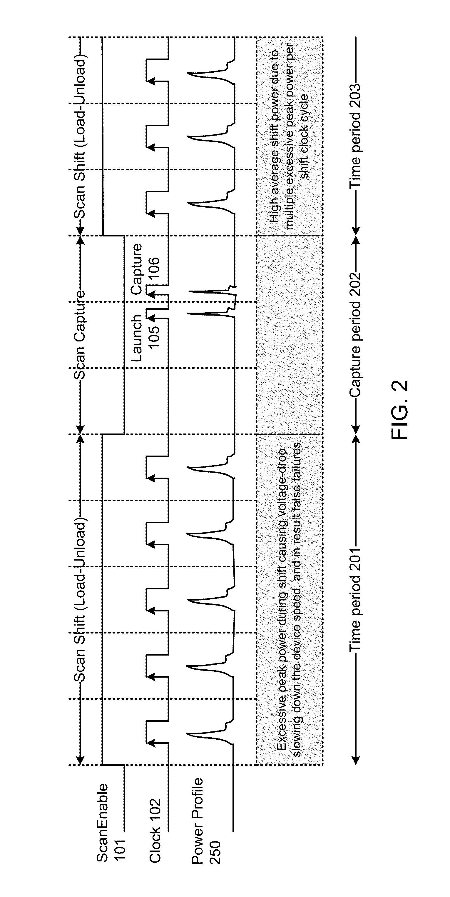
[0012]Accordingly, a need exists for a system that allows scan capture operations to run at the high clock speeds while reducing peak power during at-speed (e.g., at application speed) capture cycles without any coverage impact and minimal test-time impact. It is also necessary to make the scan test mode power-aware to avoid stressing the power distribution network in test mode during production testing. Embodiments of the present invention provide a method and system for reducing peak power problems during scan capture mode that are computationally efficient and provide high defect coverage.

Problems solved by technology

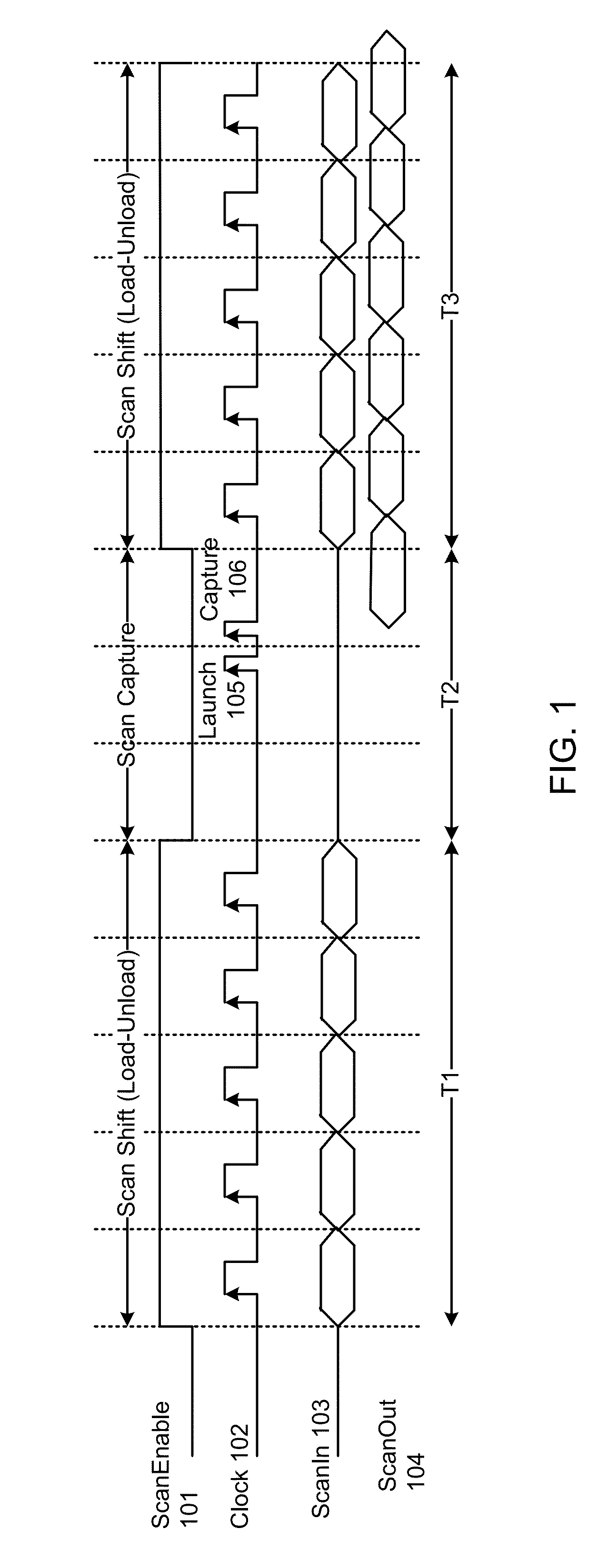
Scan based tests are expensive because of the high capital investment in test equipment and because they can require a considerable amount of time to run.
However, it can cause power issues resulting in flip-flops and gates behaving incorrectly under inadequate power supply conditions.
This could cause false failures due to the electrical and thermal stressing of the silicon under test, which could result in significant yield loss.
Accordingly, users of the test system are left with no other alternative but to slow down the clock speeds in order to minimize power related issues, which results in longer test times.
Further, the dynamic power consumption during scan test, with and without test compression, is always higher than the functional mode because of very high toggling rates and logic activity during scan shift and scan capture operations and can result in excessive heat dissipation during testing that can damage the package.
This increased dynamic power consumption can cause reliability issues in chips, which may result in the chip subsequently failing in the field.
This is because during scan test mode, power dissipation will exceed the peak power for which the chip and package has been designed.
Certain conventional systems have attempted to address power reduction during scan capture cycles, but they are either costly in terms of computation time or require significant implementation and verification efforts.
However, this technique requires considerable memory and CPU resources.
However, these methods also are problematic because they lead to lower defect coverage than random-fill.
This technique is efficient because it prevents the ATPG tool from performing too many computations, and it is faster in terms of run time, however, significant implementation and verification efforts are required to implement it and there is considerable logic overhead.

Method used


Image

  • Global low power capture scheme for cores
  • Global low power capture scheme for cores
  • Global low power capture scheme for cores

Examples


Embodiment Construction

[0032]Reference will now be made in detail to the various embodiments of the present disclosure, examples of which are illustrated in the accompanying drawings. While described in conjunction with these embodiments, it will be understood that they are not intended to limit the disclosure to these embodiments. On the contrary, the disclosure is intended to cover alternatives, modifications and equivalents, which may be included within the spirit and scope of the disclosure as defined by the appended claims. Furthermore, in the following detailed description of the present disclosure, numerous specific details are set forth in order to provide a thorough understanding of the present disclosure. However, it will be understood that the present disclosure may be practiced without these specific details. In other instances, well-known methods, procedures, components, and circuits have not been described in detail so as not to unnecessarily obscure aspects of the present disclosure.

[0033]S...


PUM


Abstract

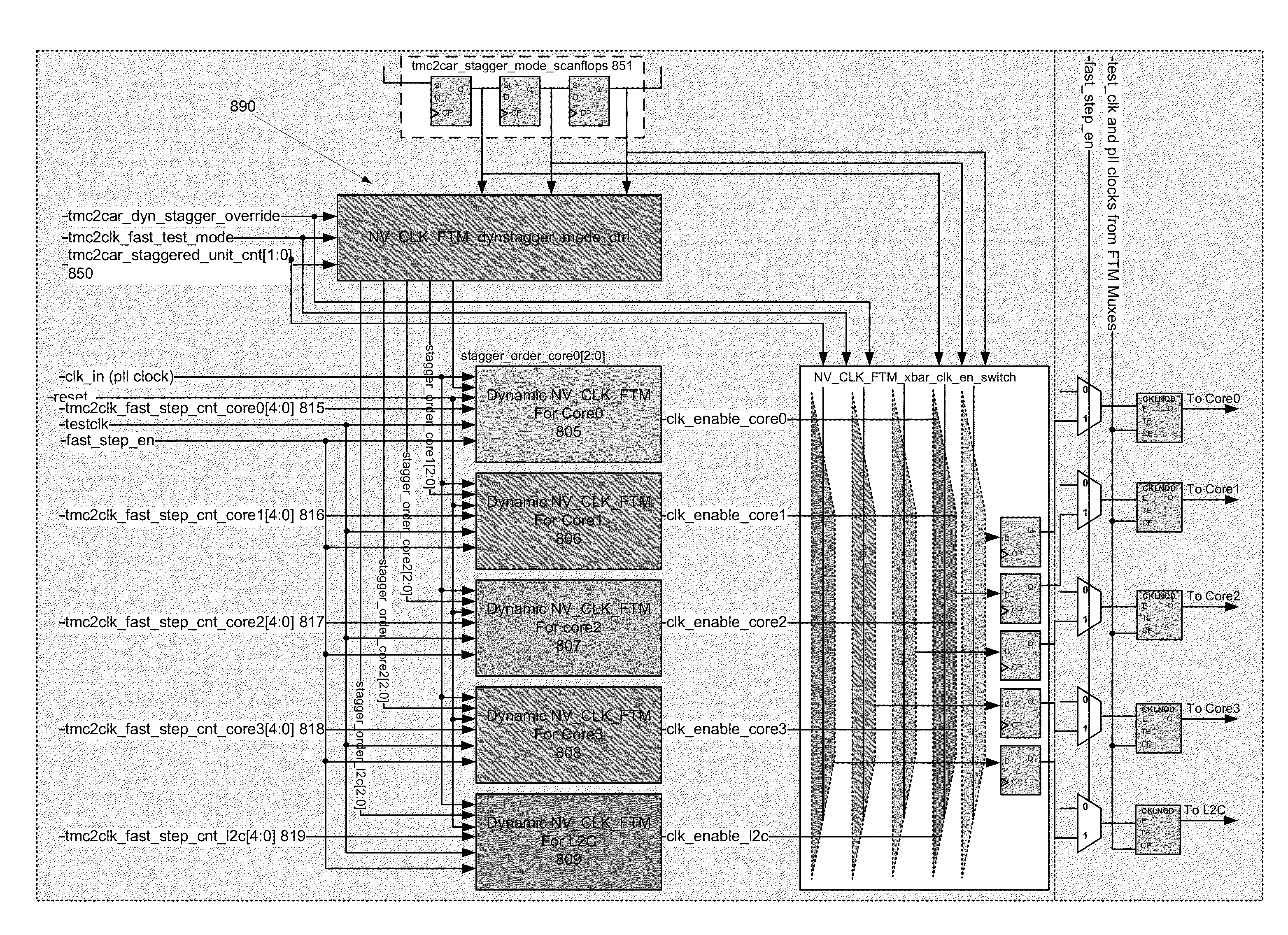
A method for testing an integrated circuit to reduce peak power problems during scan capture mode is presented. The method comprises programming a respective duration of a first time window for each of a plurality of cores and a cache on the integrated circuit. It further comprises counting the number of pulses of a first clock signal during the first time window for each of the plurality of cores and the cache. Subsequently, the method comprises staggering capture pulses to the plurality of cores and the cache by generating pulses of a second clock signal for each of the plurality of cores and the cache during a respective second time window, wherein the number of pulses generated is based on the respective number of first clock signal pulses counted for each of the plurality of cores and the cache.

Description

CROSS-REFERENCE T0 RELATED APPLICATIONSRelated Applications[0001]The present application is related to U.S. Pat. No. 7,305,598, filed Mar. 25, 2005, entitled “TEST CLOCK GENERATION FOR HIGHER-SPEED TESTING OF A SEMICONDUCTOR DEVICE,” naming Amit Sanghani and Philip Manela as inventors. That application is incorporated herein by reference in its entirety and for all purposes.[0002]The present application is also related to the following co-pending U.S. patent applications: U.S. patent application Ser. No. ______, filed ______, entitled “SYSTEM FOR REDUCING PEAK POWER DURING SCAN SHIFT AT THE LOCAL LEVEL FOR SCAN BASED TESTS,” naming Milind Sonawane, Satya Puvvada and Amit Sanghani as inventors, and having attorney docket number NVID-PSC-11-0240-US1, which is incorporated herein by reference in its entirety and for all purposes, U.S. patent application Ser. No. ______, filed ______, entitled “SYSTEM FOR REDUCING PEAK POWER DURING SCAN SHIFT AT THE GLOBAL LEVEL FOR SCAN BASED TESTS,” n...

Claims


Application Information

Patent Timeline
Patent Type & Authority Applications(United States)
IPC IPC(8): G01R31/3177
CPCG01R31/3177G01R31/318544G01R31/318575
Inventor PUVVADA, SATYASONAWANE, MILINDSANGHANI, AMIT D.SINHA, ANUBHAVAGARWAL, VISHAL
Owner NVIDIA CORP
Why Eureka
Try Eureka