MEMS mass flow sensor assembly and method of making the same

a technology of mass flow sensor and assembly method, which is applied in the direction of volume/mass flow measurement, measurement device, instrument, etc., can solve the problems of affecting the flow stability of the sensor, and the inability to meet the requirements of the measurement. , to achieve the effect of reducing the size of the sensor, avoiding the bump, and minimizing the flow instability

Active Publication Date: 2014-07-10
M TECH INSTR HLDG
View PDF4 Cites 14 Cited by
  • Summary
  • Abstract
  • Description
  • Claims
  • Application Information

AI Technical Summary

Benefits of technology

[0008]It is the objective of this invention to design a process as well as the package assembly for the MEMS mass flow sensors utilizing the thermal calorimetric principle and the sensing elements are placed on the front side of the silicon wafer surface with the supportive membrane made of silicon nitride or polymers. The preferred MEMS mass flow sensor shall be free of the front side wire binding configuration such that the major reliability due to wire failure could be eliminated while the flow instability shall be minimized by eliminating the bumps created by the sealing of the wires interface between the MEMS chip and the control electronics. The invented design shall also maintain a minimal footprint required for the said MEMS mass flow sensors for cost considerations. The process of the said sensor assembly shall further provide the fully automation approaches in order to meet the objectives of manufacturability and flexibility.

Problems solved by technology

MEMS mass flow sensors for gases have been limited to clean and dry gases, partly due to the design limitation of the most available products on market.
Consequently, the wire connection between the device and the interface has to be exposed to the gas medium resulting in a volatile and fragile nature against fluids that may contain moisture, other conductive dilute mist, and particle, since these materials can lead to a shortage of the wire or even a destruction of the whole device.
Further high speed flow pulsed flow may also create unpredictable damages to the connection wires or the devices as a whole.
But the configuration also requires that the electronic control circuitry be effective sealed from the contact of the flow medium otherwise it would at least add large noises and other unexpected instabilities.
This again limited the applications for fluid in a larger pipeline while adding possible pressure loss in the main flow channel in order to drive the gas medium into the bypass sensing configurations.
(Ueda, N. and Nozoe, S., Flow rate measuring device, US Patent Application 2008 / 0314140) and Fujiwara et al., (Fujiwara, T.; Nozoe, S. and Ueda, N., Flow velocity measuring device, U.S. Pat. No. 7,062,963) to avoid the clogging of particles in the small bypass channels however did not change the basic package landscape of the bypass configuration, and the complicated channel design might only improves the failure rate of particle impact but the damages due to the presence of the liquid is still an unsolved issue.
Nonetheless, such a configuration shall create an unavoidable scaling hump on the MEMS chip front surface for which the bump shape is usually difficult to control, which would also be undesirable for maintaining the stability for the flow medium passing through the front MEMS chip surface.
These processes are both time consuming and might also incur additional reliability uncertainties due to the sealing materials stress release, false soldering during wire binding, as well as leakage of the sealing.

Method used


Image

  • MEMS mass flow sensor assembly and method of making the same
  • MEMS mass flow sensor assembly and method of making the same
  • MEMS mass flow sensor assembly and method of making the same

Examples


Embodiment Construction

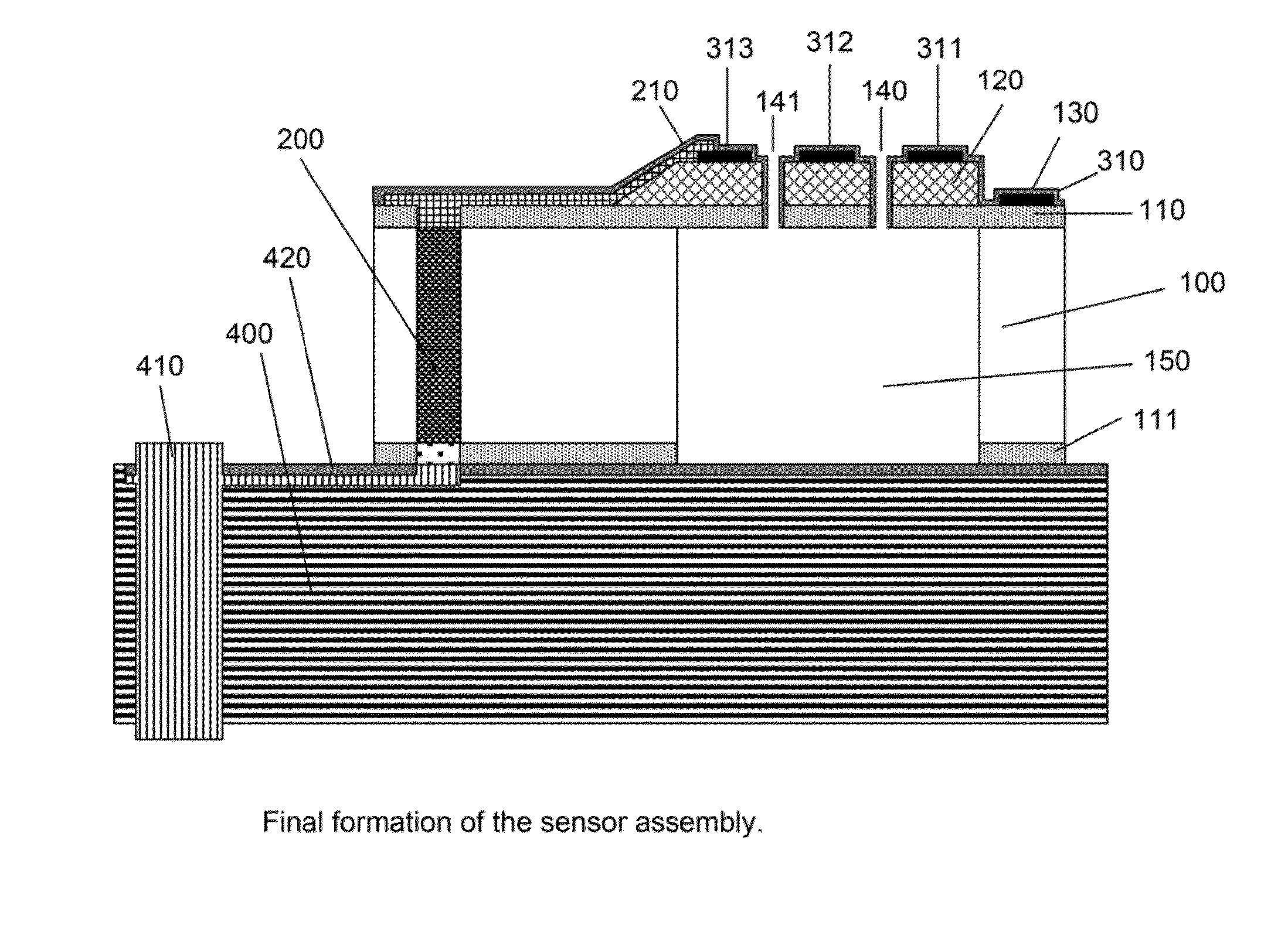
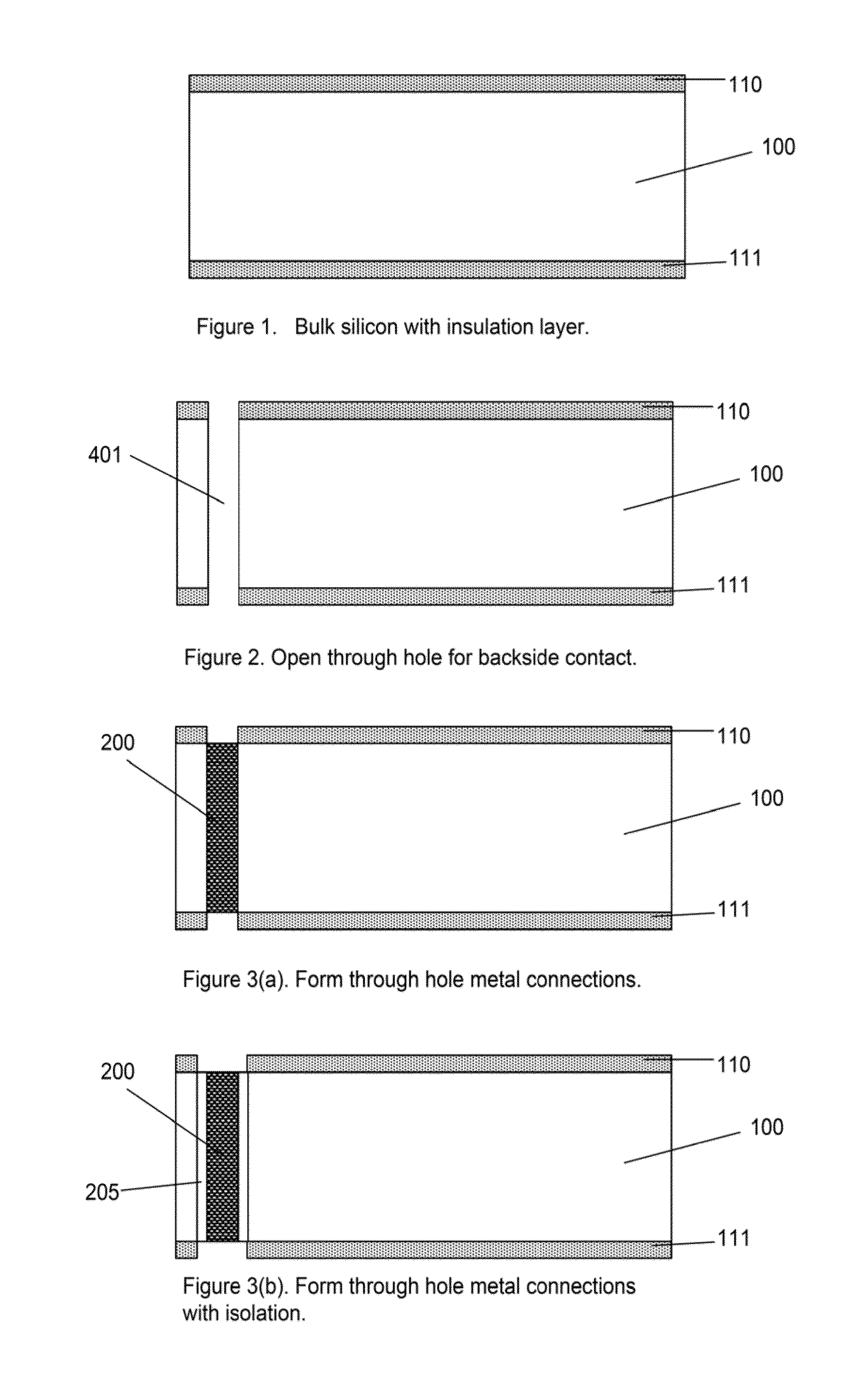
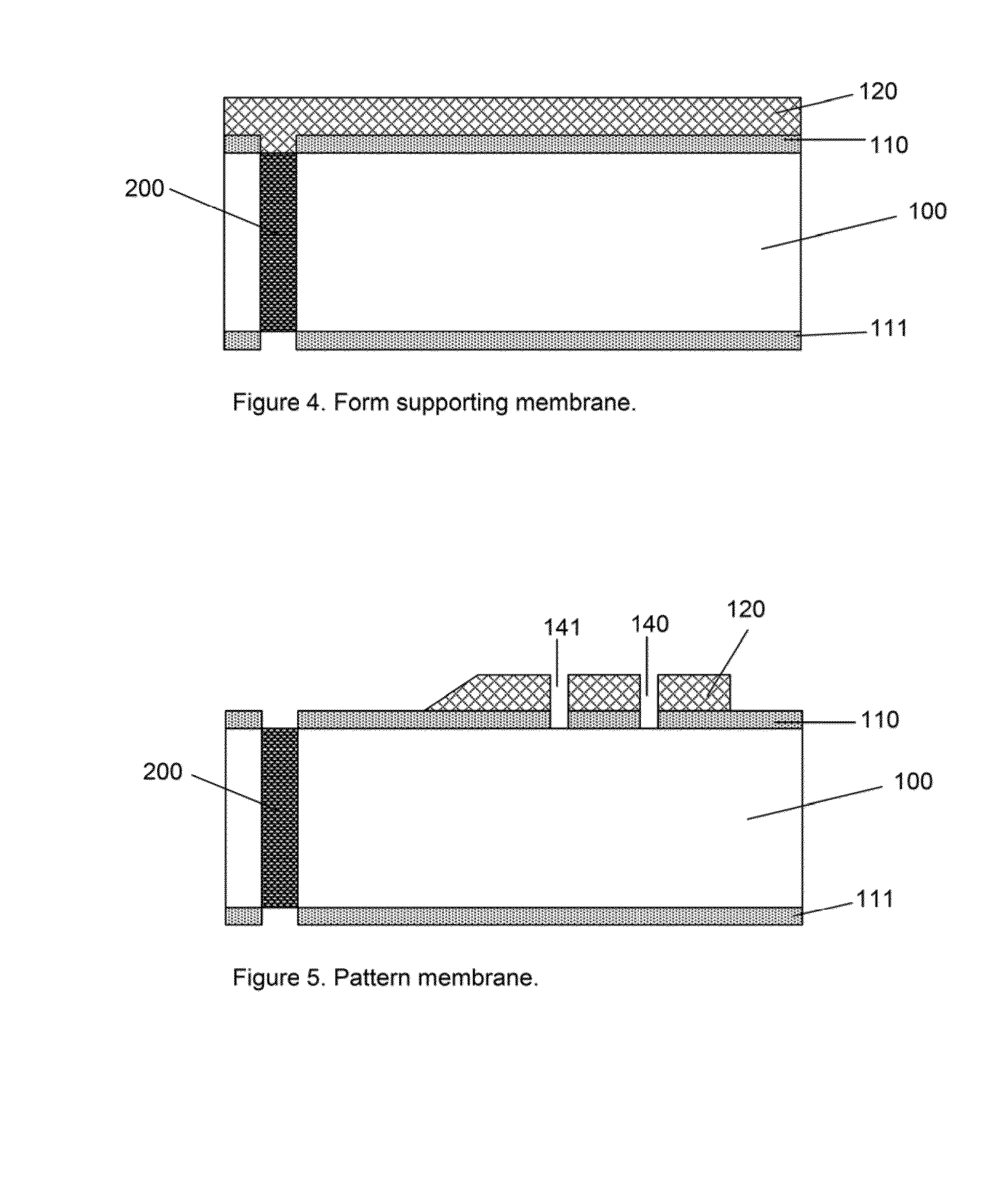
[0029]The preferred MEMS mass flow sensor assembly starts with sensor manufacture on a silicon substrate (100) or silicon water as shown in FIG. 1. The preferred silicon substrate is of high electrical conductivity either heavily doped with phosphorus or boron but preferred to be heavily doped with boron. The silicon substrate is further preferred to be non-electrical conductive without any doping. The silicon substrate is passivated using silicon nitride (110 and 111) at its both surfaces using low pressure chemical vapor deposition. The thickness of the silicon nitride should be from 100 to 300 nm but preferably 200 nm.

[0030]The preferred MEMS mass flow sensor is then proceed to open the through wafer conductive pathways and the pre-designed locations (401). For several viable processes, the pathways could be through the silicon substrate as shown in FIG. 2. Or alternatively it can be made half way through while the remaining on through-hole portions could be later removed using c...


PUM


Abstract

A silicon mass flow sensor manufacture process that enables the backside contacts and eliminates the conventional front side wire binding process, and the assembly of such a mass flow sensor is disclosed in the present invention. The achieved assembly enhances the reliability by eliminating the binding wire exposure to the flow medium that may lead to detrimental failure due to the wire shortage or breakage while the miniature footprint could be maintained. The assembly further reduces flow instability from the flow sensor package including the bump of wire sealing. The invented mass flow sensor assembly can be a flow sensor module if the supporting sensor carrier is pre-designed with the control electronics. Without the control electronics, the said mass flow sensor assembly is easy to install into desired flow channels and connect to the external control electronics.

Description

[0001]We claim the priority to US provisional application Ser. No. 61 / 585,908, filed on Jan. 12, 2012.BACKGROUND OF THE INVENTION[0002]1. Field of the Invention[0003]This invention relates to micromachined silicon sensors or Micro Electro Mechanical Systems (MEMS) mass flow sensing technology that minimizes the disturbance around the sensor chip due to the connection of wires. This invention also provides the enhanced reliability that eliminates the sensor malfunction or damage due to the short or destruction of the exposed connection wires between the sensor chip and its carrier. The present invention further facilitates the automation process of the sensor module manufacture. This invention additionally reduces the cost of the sensor module manufacture with the reduction of wire binding of the sensor chip to its carrier and sealing process.[0004]2. Description of the Related Art[0005]MEMS mass flow sensors for gases have been limited to clean and dry gases, partly due to the desig...

Claims


Application Information

Patent Timeline
Patent Type & Authority Applications(United States)
IPC IPC(8): G01F1/69
CPCG01F1/69G01F1/684G01F1/6845G01F1/692
Inventor HUANG, LIJICHEN, CHIH-CHANG
Owner M TECH INSTR HLDG
Why Eureka
Try Eureka