Airgap interconnect with hood layer and method of formiing

Active Publication Date: 2014-07-10
TAHOE RES LTD
View PDF2 Cites 26 Cited by
  • Summary
  • Abstract
  • Description
  • Claims
  • Application Information

AI Technical Summary

Problems solved by technology

As microprocessors become faster and smaller, integrated circuitry (IC) becomes more complex and components become more densely packed.
However, the dielectric properties of the substrate material enable capacitive coupling between adjacent interconnects, which increases chip power requirements and interferes with signal transmission.
As device dimensions decrease, interconnect

Method used


Image

  • Airgap interconnect with hood layer and method of formiing
  • Airgap interconnect with hood layer and method of formiing
  • Airgap interconnect with hood layer and method of formiing

Examples


Embodiment Construction

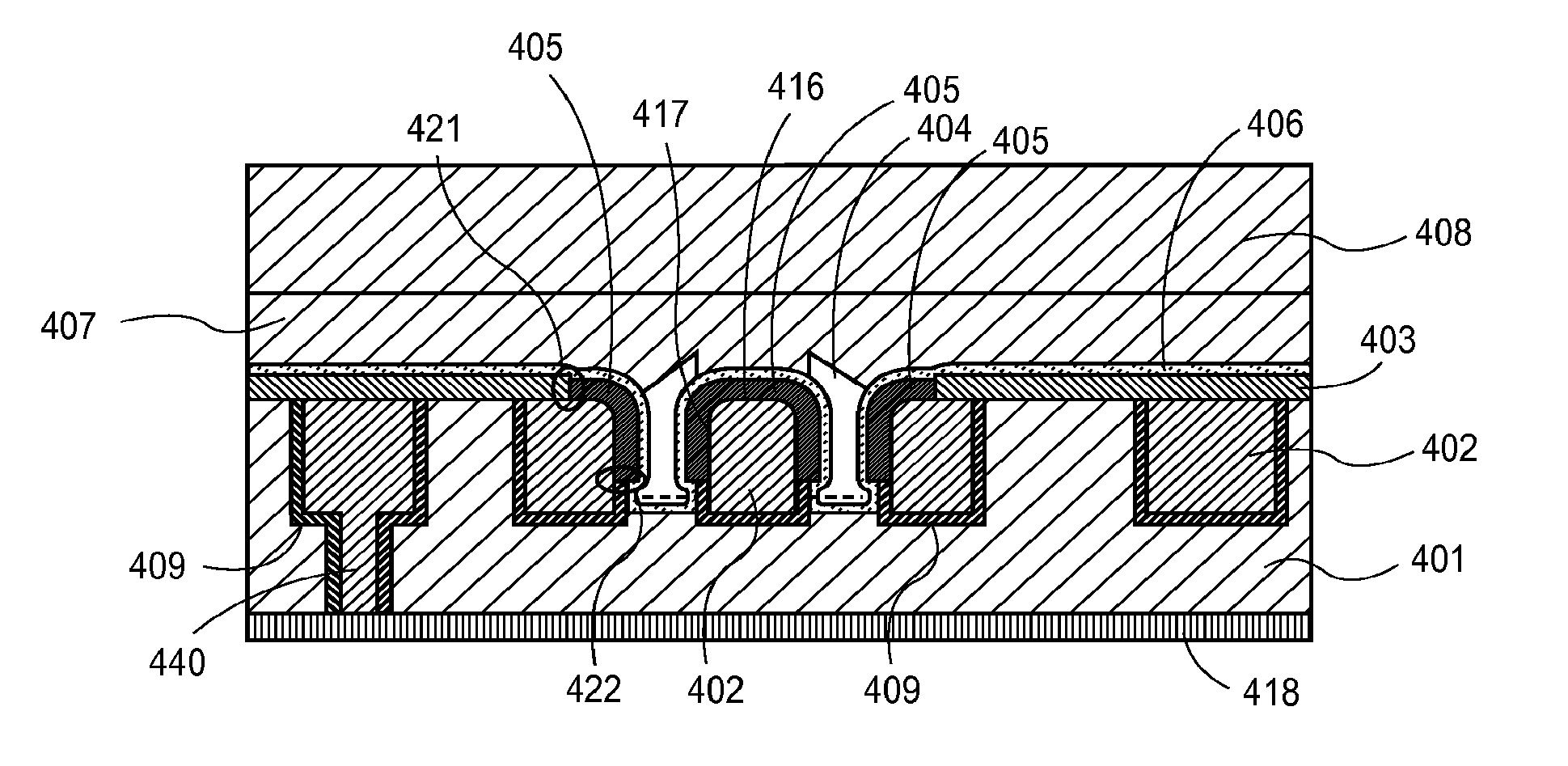
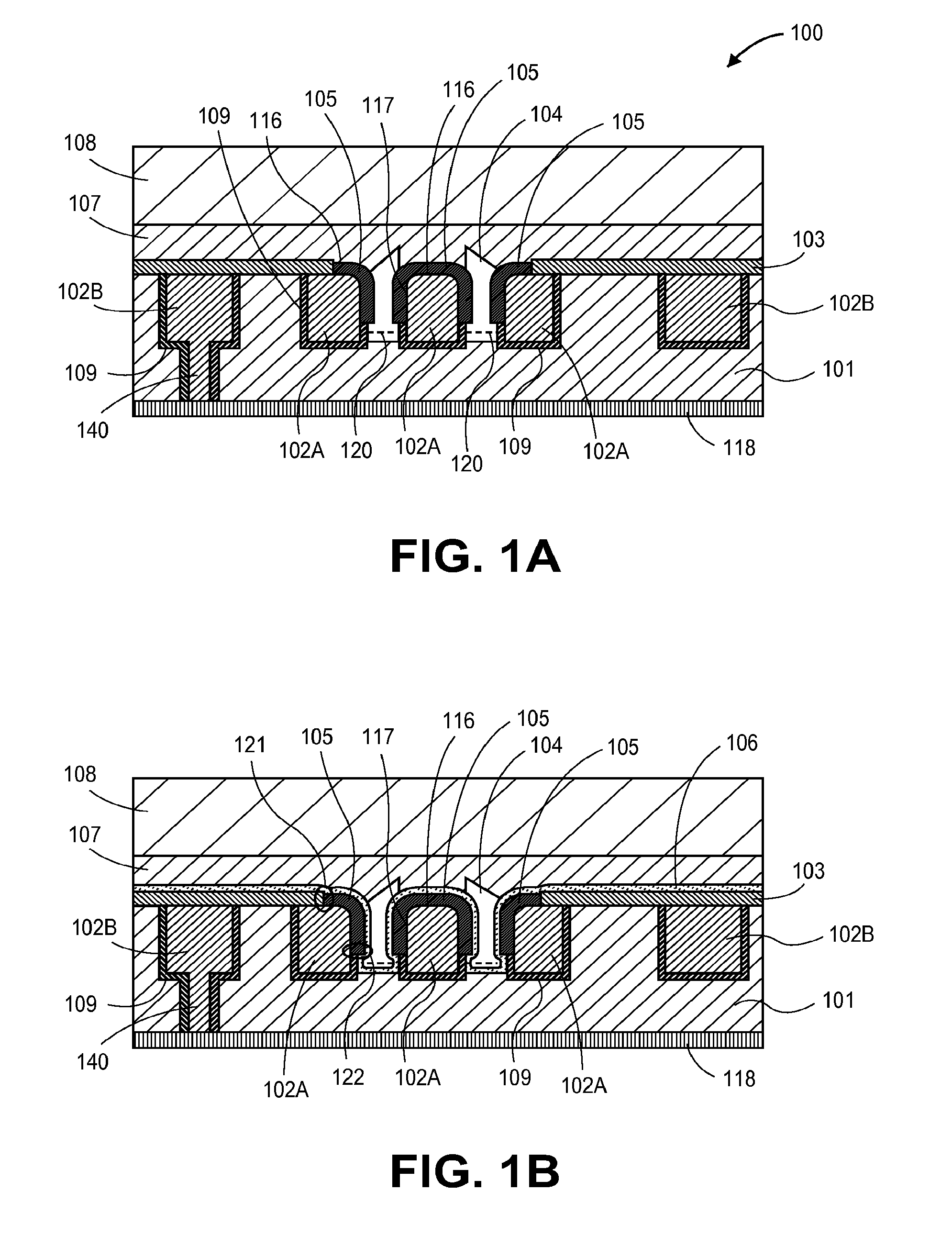
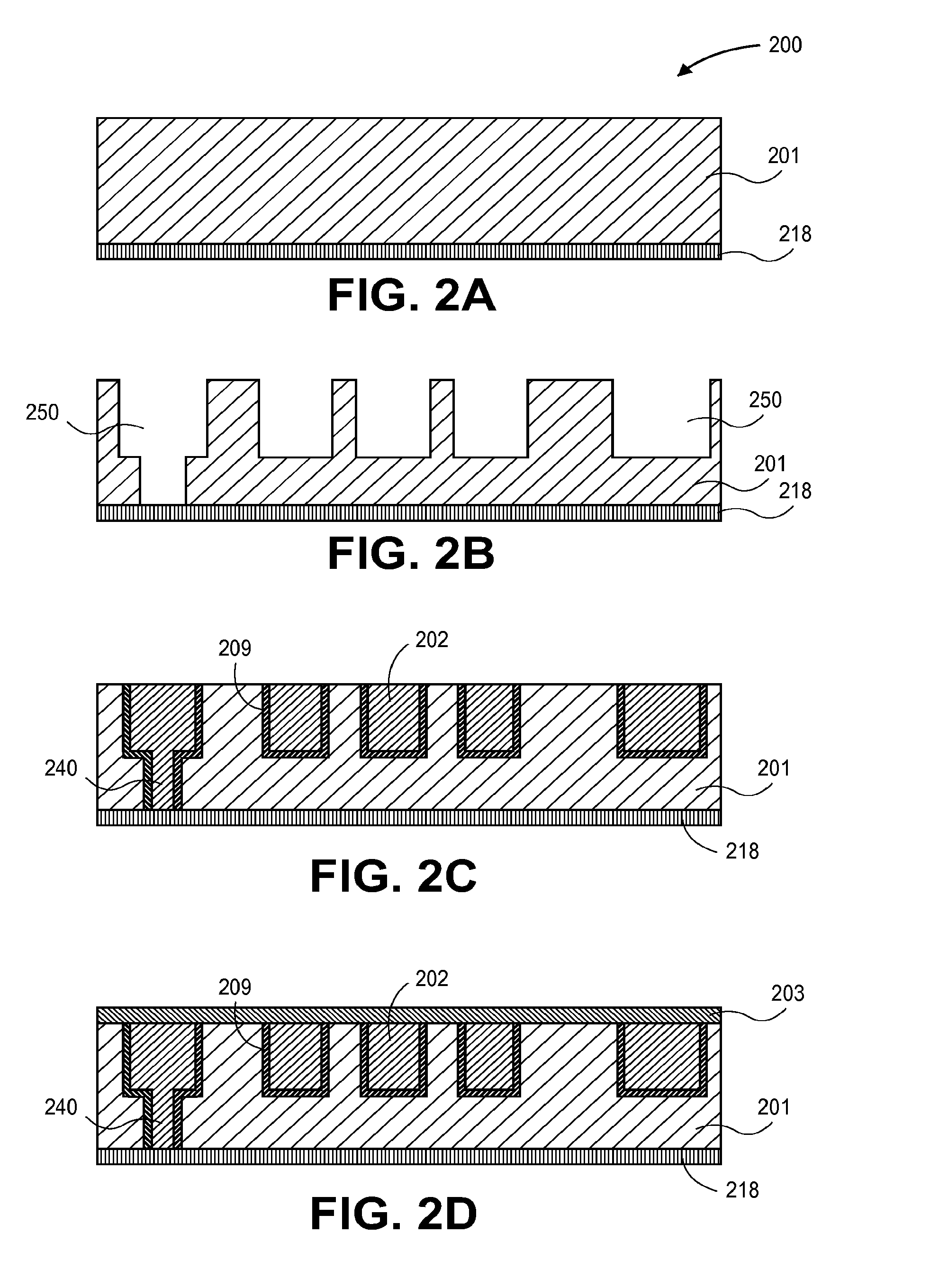
[0014]An airgap interconnect structure with a hood layer for use in an integrated circuit and a process for forming such airgap interconnects with hood layer are described. Embodiments of the present invention have been described with respect to specific details in order to provide a thorough understanding of the invention. One of ordinary skill in the art will appreciate that the invention can be practiced without these specific details. In other instances, well known semiconductor processes and equipment have not been described in specific detail in order to not unnecessarily obscure the present invention. Additionally, the various embodiments shown in the figures are illustrative representations and are not necessarily drawn to scale.

[0015]An airgap interconnect structure with a hood layer and methods for forming such airgap interconnects with hood layers are disclosed herein. Interconnect surfaces must be sealed by one or more barrier layers to prevent diffusion of the interconn...


PUM


Abstract

An airgap interconnect structure with hood layer and methods for forming such an airgap interconnect structure are disclosed. A substrate having a dielectric layer with a plurality of interconnects formed therein is provided. Each interconnect is encapsulated by a barrier layer. A hardmask is formed on the dielectric layer and patterned to expose the dielectric layer between adjacent interconnects where an airgap is desired. The dielectric layer is etched to form a trench, wherein the etching process additionally etches at least a portion of the barrier layer to expose a portion of the side surface of each adjacent copper interconnect. A hood layer is electrolessly plated onto an exposed portion of the top surface and the exposed portion of the side surface to reseal the interconnect. A gap-sealing dielectric layer is formed over the device, sealing the trench to form an airgap.

Description

FIELD OF THE INVENTION[0001]The present invention relates generally to the manufacture of semiconductor devices. In particular, embodiments of the present invention relate to airgap interconnects with a hood layer that prevents diffusion and electromigration of the interconnect material to increase interconnect reliability.BACKGROUND AND RELATED ARTS[0002]As microprocessors become faster and smaller, integrated circuitry (IC) becomes more complex and components become more densely packed. IC components are connected by conductive traces and vias (collectively referred to as “interconnects”) though which electrical signals are sent and / or received. Interconnects are typically formed through a damascene process, whereby conductive material is deposited into holes and trenches etched into a semiconductor substrate. The surrounding material electrically insulates each interconnect from neighboring interconnects. However, the dielectric properties of the substrate material enable capacit...

Claims


Application Information

Patent Timeline
IPC IPC(8): H01L23/532H01L21/768
CPCH01L21/7685H01L23/53238H01L23/5222H01L21/76852H01L21/7682H01L21/76834H01L23/53295H01L21/764H01L2924/00H01L2924/0002
Inventor FISCHER, KEVIN
Owner TAHOE RES LTD
Why Eureka
Try Eureka