

Integrated charge production architecture
a charge production and integrated technology, applied in the field of renewable energy production, can solve the problems of emission within the high surface area basal plane of nanowires, and achieve the effects of reducing the amount of radiation, broad spectrum absorption and charge production, and rapid charge separation and transportation
Inactive Publication Date: 2014-07-17
GRIMES CRAIG +2
View PDF1 Cites 7 Cited by
- Summary
- Abstract
- Description
- Claims
- Application Information
AI Technical Summary
Benefits of technology
The present invention is about making better use of radiation than existing systems. One method involves depositing titanium dioxide on a substrate without using an electrochemical reaction. In this invention, there is a vertical structure made up of nanowires and quantum dots that can absorb a broad range of radiation and produce electricity. This structure also allows for the separation and transport of charges quickly, reducing recombination and associated losses. The invention also minimizes thermalization, which means reducing the amount of heat that is generated. This is done by quickly extracting more electricity and using heat from external sources to produce even more electricity.
Problems solved by technology
Further, thermal energy absorbed by such an architecture can result in emissions within the high surface area basal plane of the nanowires (e.g., from nanowire to nanowire) for absorption and further charge production by the architecture.
Method used
View moreImage
Smart ImageViewing Examples


Examples
example 1
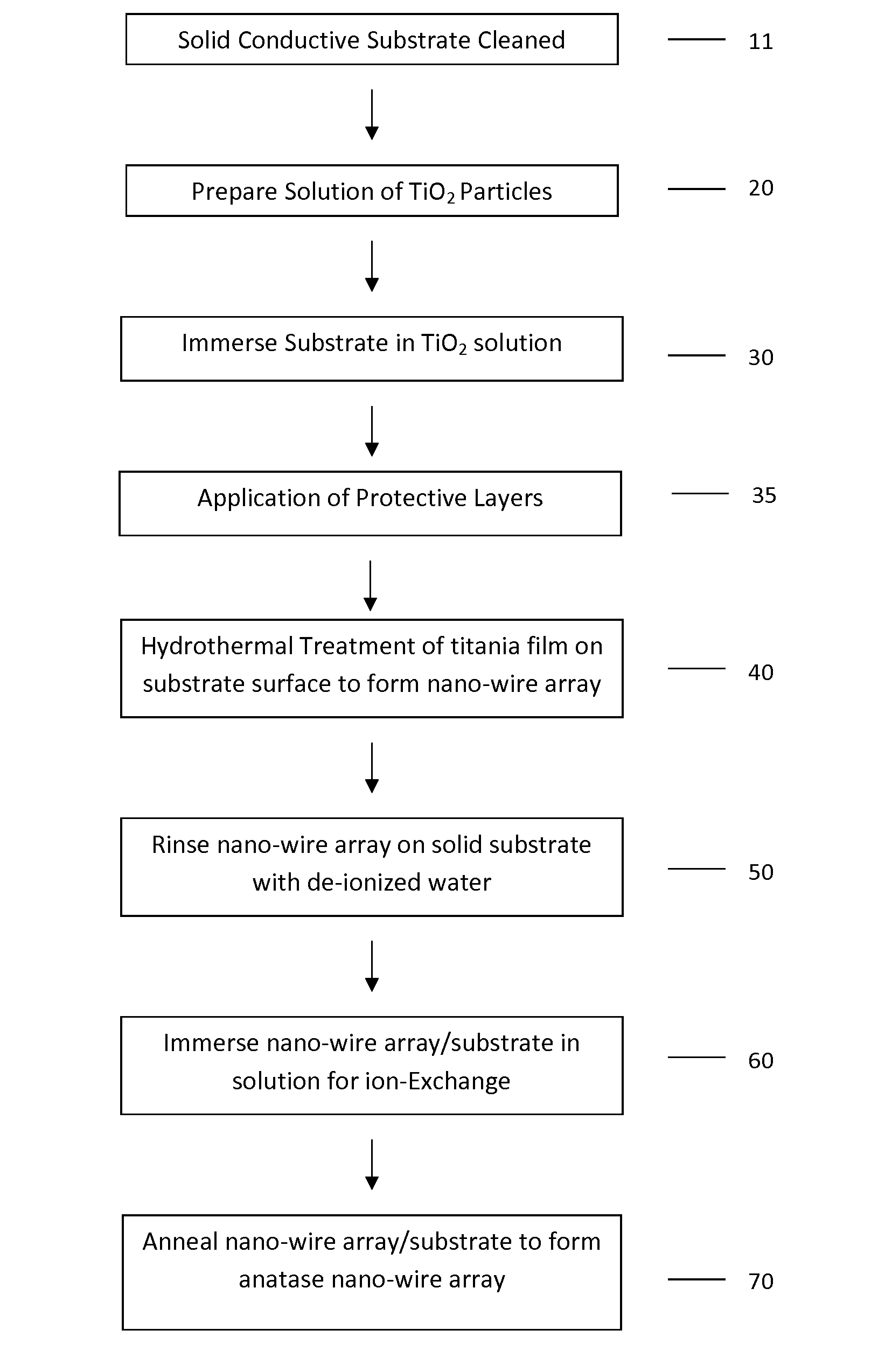
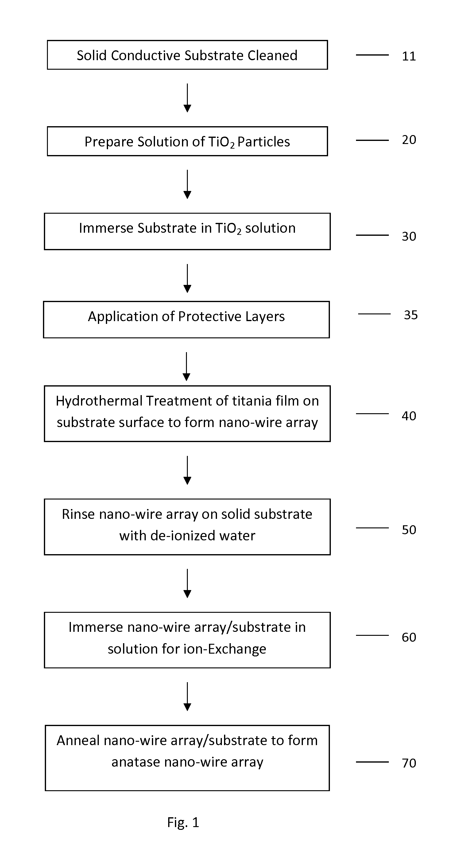
[0154]A Ti02 solution can be made using 0.1 g to 0.4 g of P25 nanoparticles in 10 ml of solvent which can be, for example, 3 ml titanium tert-butoxide in 7 ml ethanol. Solution dispersion is enhanced by stirring for an extended period, approximately 5-20 min. A FTO-glass substrate, was immersed in the Ti02 solution between 30 seconds and 180 minutes, and more preferably between 3 min and 60 min. After deposition of the several micron thick Ti02 film, the substrate was taken out from the solution and annealed at 500° C. for 1 h to remove any residual organics. After this step, a protective Teflon coating was sprayed onto the back (non-TCO covered side) of the glass substrate.
Login to View More PUM
| Property | Measurement | Unit |
|---|---|---|
| temperatures | aaaaa | aaaaa |
| wavelengths | aaaaa | aaaaa |
| wavelengths | aaaaa | aaaaa |
Abstract
The present invention relates to fabrication and application of compositions, devices, methods and systems for utilizing radiation more efficiently as compared to known systems. A synthesis method provides deposition of titania on a substrate without the use of an electrochemical reaction. An integrated architecture formed by the method of the present invention is comprised of vertically-oriented, one-dimensional, monocrystalline, n-type anatase nanowires in communication with a common transparent conductive substrate, and which are intercalated with a consortia of p-type quantum dots tuned for absorption of infrared and other radiation.
Description
CROSS REFERENCE TO RELATED APPLICATION[0001]This application is a continuation in part of U.S. patent application Ser. No. 13 / 590,786 and claims the benefit of U.S. Provisional Patent Application No. 61 / 792,783, filed Mar. 15, 2013, the entirety of each of the applications is hereby incorporated by reference into this application.BACKGROUND OF THE INVENTION[0002]1. Field of the Invention[0003]The present invention relates to renewable energy production, as well as devices, methods, compositions, systems and other means for manufacturing and using an integrated architecture for charge production from radiation and thermal energy.[0004]2. Description of Related Art[0005]Heat is considered to be a form of waste in a vast array of devices and processes in myriad industries and applications (e.g., transportation, heat and power production, manufacturing and electronics). Microprocessors, for example, generate heat as they consume electrical energy to perform their intended functions. Suc...
Claims
Login to View More Application Information
Patent Timeline
 Patent Type & AuthorityApplications(United States)
IPC IPC(8): C30B1/10C30B1/02
CPCC30B1/02C30B1/10H01L29/0665H01L29/0676H01G9/2031C30B7/10C30B29/34B01J37/0228B01J37/033B01J37/06B01J37/346B01J37/348B01J21/063H01L29/127B82Y10/00C30B29/602B01J35/30B01J35/39B01J35/58
InventorGRIMES, CRAIGLATEMPA, THOMASKREISLER, KEVIN
OwnerGRIMES CRAIG