Switching regulator including charge pump

Inactive Publication Date: 2014-07-17
RICHTEK TECH
View PDF1 Cites 1 Cited by
  • Summary
  • Abstract
  • Description
  • Claims
  • Application Information

AI Technical Summary

Benefits of technology

[0008]From one perspective, the present invention provides a switching regulator, for converting an input voltage to an output voltage, the switching regulator including: a power stage circuit, for switching at least one power switch thereof according to a driving signal to convert the input voltage to the output voltage, the power stage circuit including: an active circuit, which includes the power switch and an inductor, the active circuit being c

Problems solved by technology

Besides, when the output voltage Vout is high, the inductor current of t

Method used


Image

  • Switching regulator including charge pump
  • Switching regulator including charge pump
  • Switching regulator including charge pump

Examples


first embodiment

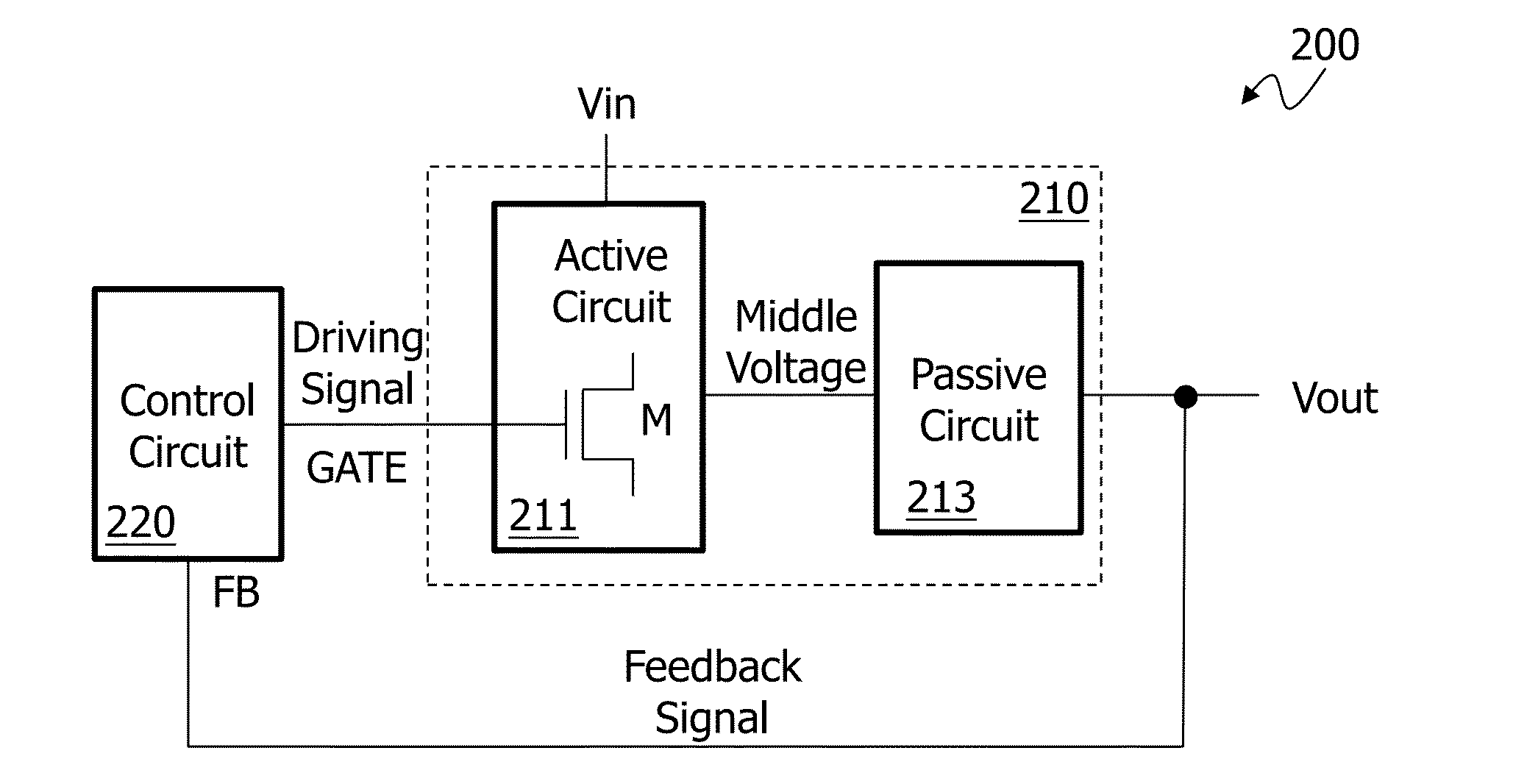
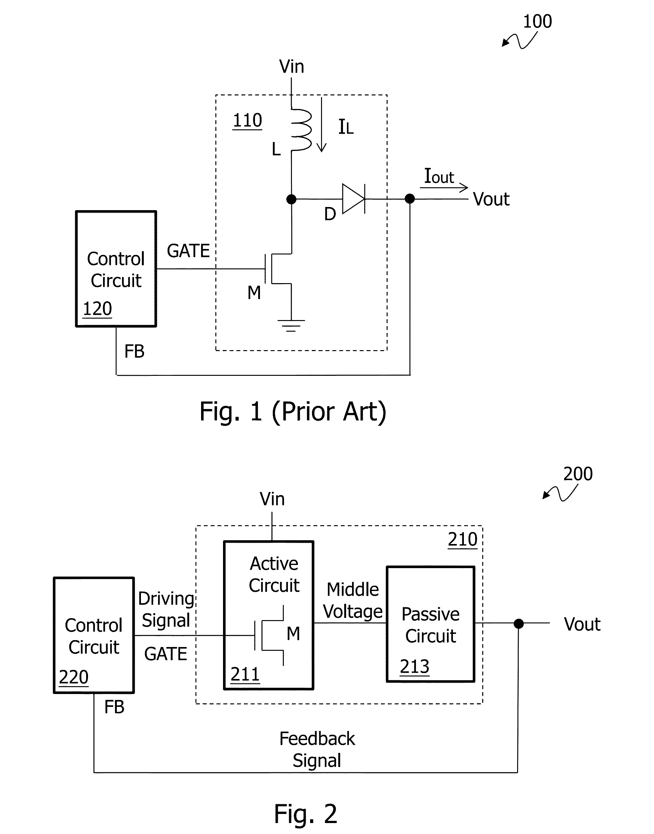
[0026]FIG. 2A shows the present invention. As shown in FIG. 2A, a switching regulator 200 includes a power stage circuit 210 and a control circuit 220. The power stage circuit 210 switches a power switch M according to a driving signal GATE to convert an input voltage to an output voltage Vout. The control circuit 220 is coupled to the power stage circuit 210, and generates the driving signal GATE according a feedback signal. The power stage circuit 210 includes an active circuit 211 and a passive circuit 213. The active circuit 211 includes the power switch M and an inductor (not shown, to be described in detail later). The active circuit 211 is for receiving the input voltage Vin and the driving signal GATE to convert the input voltage Vin to a middle voltage. The passive circuit 213 is coupled to the active circuit 211, and includes a charge pump (not shown, to be described in detail later) to convert the middle voltage to the output voltage Vout. The active circuit 211 is for ex...

second embodiment

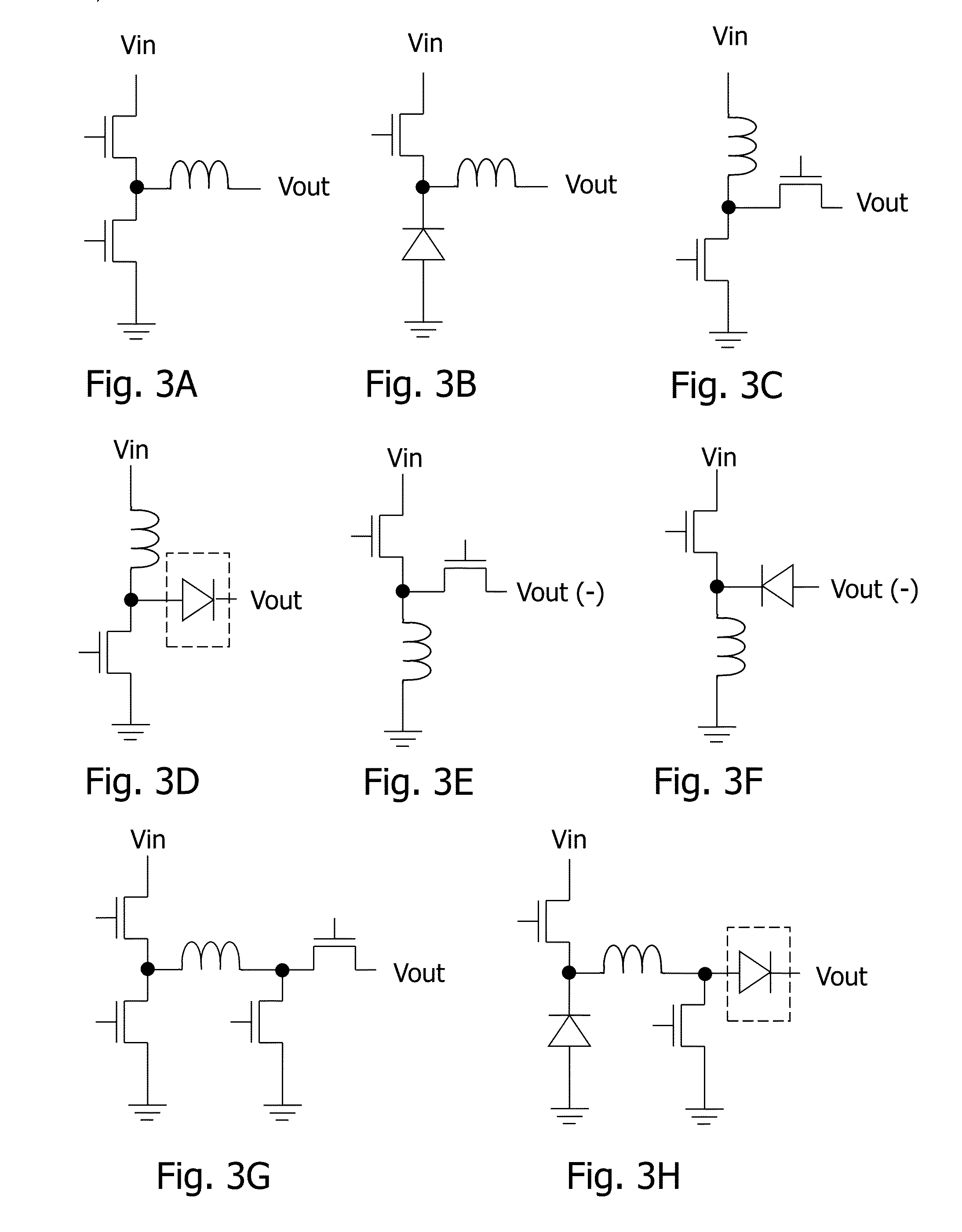
[0027]FIG. 4 shows the present invention. This embodiment shows a more specific structure of the switching regulator 200 according to the present invention. As shown in the figure, the active circuit 211 includes the aforementioned boost power stage circuit, which includes the power switch M1, an inductor L1, and a diode D1. The passive circuit 213 includes a capacitor C1 and diodes D1 and D2, wherein the capacitor C1 and the diodes D1 and D2 form the charge pump, i.e., the charge pump includes the capacitor C1, and the diodes D1 and D2. The capacitor C1 has one end coupled to a node between the power switch M1 and the inductor L1. The diode D1 has a forward terminal coupled to the other end of the capacitor C1, and a reverse terminal coupled to the output voltage Vout. The diode D2 has a forward terminal for receiving a voltage, and a reverse terminal coupled to the other end of the capacitor C1, wherein the voltage may be the aforementioned input voltage Vin1 or another predetermi...

third embodiment

[0031]FIG. 5 shows the present invention. This embodiment shows another more specific structure of a switching regulator 300 according to the present invention. As shown in FIG. 5, the active circuit 311 includes another form of the boost power stage circuit, which has the power switch M1, the inductor L1, and the diode D2; and the passive circuit 213 includes the capacitor C1, and the diodes D1 and D2, wherein the capacitor C1 and the diodes D1 and D2 form the charge pump. The passive circuit 213 receives the predetermined voltage Vin2, wherein the predetermined voltage Vin2 for example is not higher than the input voltage Vin1. Certainly, the predetermined voltage Vin2 may have the same level with the input voltage Vin1.

[0032]FIGS. 6A-6G show advantages of the present invention over the prior art by illustrative examples. The examples are based on the structure of the aforementioned second embodiment, wherein when the driving signal GATE turns ON the power switch M1, a current I1 ...


PUM


Abstract

The present invention discloses a switching regulator. The switching regulator converts an input voltage to an output voltage. The switching regulator includes: a power stage circuit, which switches at least one power switch thereof according to a driving signal to convert the input voltage to the output voltage; and a control circuit, which is coupled to the power stage circuit, for generating the driving signal according to a feedback signal. The power stage circuit includes: an active circuit, which includes the power switch and at least one inductor, and is controlled by a driving signal to convert the input voltage to a middle voltage; and a passive circuit, which is coupled to the active circuit, and includes a charge pump for converting the middle voltage to the output voltage.

Description

CROSS REFERENCE[0001]The present invention claims priority to U.S. 61 / 751,542, filed on Jan. 11, 2013.BACKGROUND OF THE INVENTION[0002]1. Field of Invention[0003]The present invention relates to a switching regulator including a charge pump; particularly, it relates to such switching regulator which is capable of operating with a power switch thereof having a lower withstand voltage.[0004]2. Description of Related Art[0005]FIG. 1 shows a schematic diagram of a typical switching regulator 100. As shown in FIG. 1, the switching regulator 100 includes a power stage circuit 110 and a control circuit 120. The control circuit 120 generates an operation signal GATE according to a feedback signal FB, which is related to an output voltage Vout, for operating a power switch M of the power stage circuit 110 to convert an input voltage Vin to the output voltage Vout. The power stage circuit 110 is a boost power stage circuit, which includes the power switch M, an inductor L, and a diode D. How ...

Claims


Application Information

Patent Timeline
IPC IPC(8): H02M3/156
CPCH02M3/1563H02M3/155H02M3/07
Inventor CHEN, CHING-YULIN, FENG-WEIKIM, KWANG-JAE
Owner RICHTEK TECH
Why Eureka
Try Eureka