Electromagnetic wave generation device and detection device

a detection device and electromagnetic wave technology, applied in pulse generators, electromagnetic wave modulation, pulse techniques, etc., can solve the problems of difficult to obtain a high yield, structural size limitation, and improve the efficiency of generating thz waves

Inactive Publication Date: 2014-07-17
CANON KK
View PDF2 Cites 11 Cited by
  • Summary
  • Abstract
  • Description
  • Claims
  • Application Information

AI Technical Summary

Problems solved by technology

However, they all suffer difficulty in improving the efficiency of generating THz waves and have complex configurations, and thus there is demand for semiconductor chips that can be driven electrically.
Depending on the structure of a resonator required for the oscillator, there may be problems as described below.
That is, the structural size may be limited for obtaining a resistance value required for the integrated-type shunt resistor, and the application of a modulation signal from an external power source may impose an upper limit of approximately 10 GHz by the MIM capacitor required to prevent parasitic oscillation.
Fabricating such an integrated circuit for a terahertz region, however, may require highly accurate shape control, making it difficult to obtain a high yield.

Method used


Image

  • Electromagnetic wave generation device and detection device
  • Electromagnetic wave generation device and detection device
  • Electromagnetic wave generation device and detection device

Examples


first embodiment

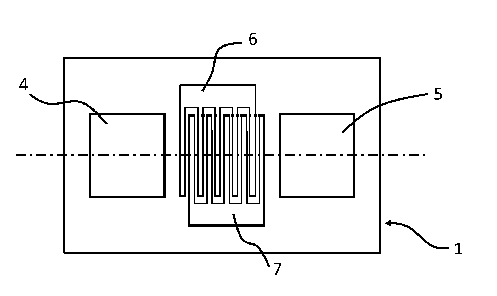
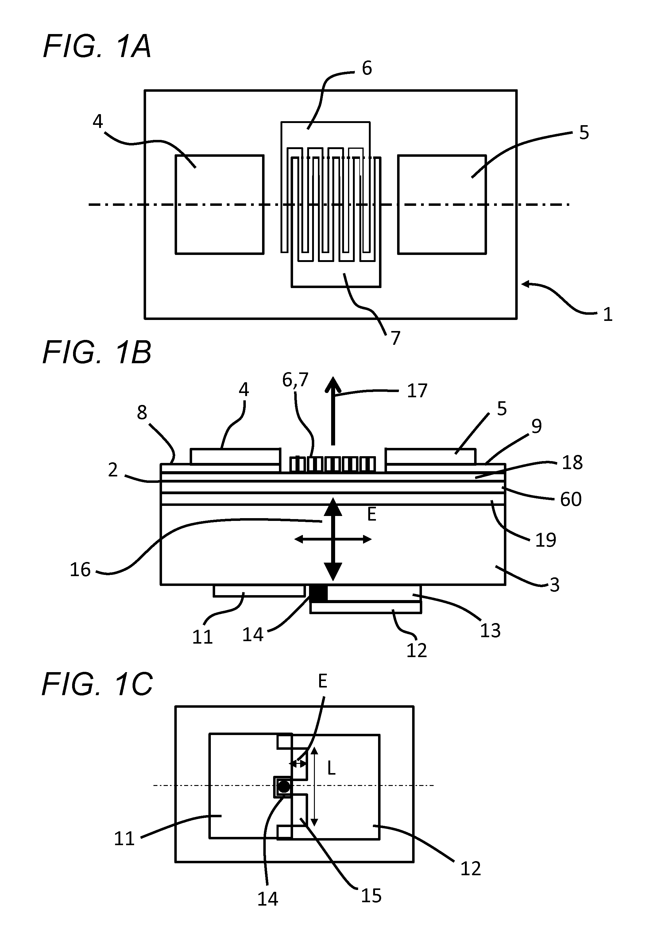
[0021]A first embodiment of the present invention provides an electromagnetic wave generation device or an oscillation device 1, which is provided with an RTD oscillator (FIG. 1C) and an HEMT device (FIG. 1A) on one substrate on its different surfaces as illustrated in FIGS. 1A to 1C. In other words, structures illustrated in FIGS. 1A and 1C in plan views are integrated on an identical substrate 3 with a cross-sectional structure illustrated in FIG. 1B in a sectional view taken along long dashed short dashed lines in the figures. The HEMT device includes grating gate electrodes 6 and 7 to be able to adjust the frequency of a plasmon occurred at a two-dimensional electron layer 2 having a semiconductor heterojunction structure. The RTD oscillator, which is a terahertz wave oscillation section including a resonant tunneling diode structure, is configured to be able to oscillate at a frequency determined by a length L of an antenna 15 provided as a resonator and an emitter. An output o...

second embodiment

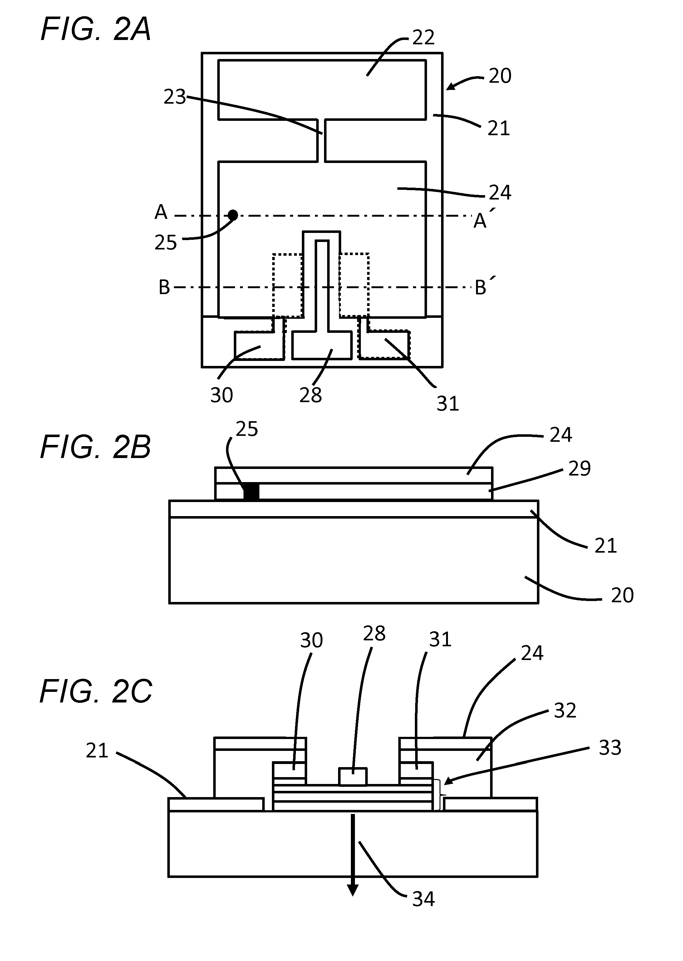
[0033]In the first embodiment, two surfaces of a substrate are used for the interaction of the RTD oscillator and the HEMT device, whereas this embodiment provides a device with the two devices integrated on an identical surface of a substrate 20. FIG. 2A is a plan view of this device, FIG. 2B is a sectional view along A-A′, and FIG. 2C is a sectional view along B-B′.

[0034]A typical arrangement of an RTD oscillator is illustrated in FIG. 2B in a sectional view. An RTD section 25 having a mesa structure as in the first embodiment and an insulator 29 are interposed between two electrodes 21 and 24. In this embodiment, an antenna provided as a resonator and an emitter is a patch antenna, and the RTD oscillator oscillates at an oscillation frequency determined by an antenna length with a bias supply line 23 as a null point. Applying a DC voltage from a power source through a pad 22 to the electrodes 21 and 24 allows the RTD oscillator to oscillate at the predetermined frequency. A stand...

third embodiment

[0038]FIG. 3 is a plan view of an oscillation device 40 according to a third embodiment, which is a modification of a structure with two devices integrated on an identical plane as with the second embodiment. In the second embodiment, which combines the RTD oscillator and the HEMT device, the oscillation output of the RTD oscillator is separated from the output of the HEMT device with difficulty. As illustrated in FIG. 3, the present embodiment is not designed to allow the output of an RTD oscillator to be emitted from an antenna to the outside, but is designed to apply the oscillation output to electrodes 49 and 50 of an HEMT device through a transmission line 44.

[0039]In an RTD oscillator with an electrode 43 serving as a resonator, an RTD section 45, as in the first and second embodiments, and an insulation film, not shown, are interposed between an electrode 42 and the electrode 43. The electrode 43 constitutes the resonator of the RTD oscillator and may be provided with a circu...


PUM


Abstract

The invention provides an electromagnetic wave generation device. The device includes a substrate provided with a terahertz wave oscillation section including a resonant tunneling diode structure, a two-dimensional electron layer having a semiconductor heterojunction structure, and a transistor section including a source electrode and a drain electrode provided at end portions of the two-dimensional electron layer and a gate electrode provided above the two-dimensional electron layer. The terahertz wave output of the terahertz wave oscillation section changes distribution of electrons in the two-dimensional electron layer.

Description

BACKGROUND OF THE INVENTION[0001]1. Field of the Invention[0002]The present invention relates to an oscillation device, a detection device, and the like, of a semiconductor, for a terahertz waveband.[0003]2. Description of the Related Art[0004]In recent years, non-destructive sensing techniques using electromagnetic waves in a terahertz (THz) waveband (at frequencies of approximately 30 GHz to 30 THz) have been developed. Electromagnetic waves in such a frequency band allow applications in imaging techniques developed in the form of safe imaging and examining apparatuses without the use of X-rays. Other techniques that have been developed include spectroscopic techniques for obtaining the absorption spectrum and the complex permittivity of a substance to determine its properties such as molecular bonding, measurement techniques for determining properties such as carrier density and mobility, conductivity, and the like, and analytic techniques for biomolecules. Additionally, the IEEE...

Claims


Application Information

Patent Timeline
Patent Type & Authority Applications(United States)
IPC IPC(8): H03B7/08
CPCH03B2200/0084H03B7/08H03B7/00H03B17/00H03C7/025H03C7/00G01J1/44H01S1/02
Inventor OUCHI, TOSHIHIKOSEKIGUCHI, RYOTA
Owner CANON KK
Why Eureka
Try Eureka