Terahertz temporal and spatial resolution imaging system, imaging method and application thereof

a technology of spatial resolution and imaging system, applied in the field of optical imaging, can solve the problems of uneven overall optical characteristics of semiconductors, scattered carriers, and spatial distribution characteristics of carriers, and achieve the effect of comprehensive and accurate observation and shortening test tim

Active Publication Date: 2014-07-17
CAPITAL NORMAL UNIVERSITY
View PDF6 Cites 21 Cited by
  • Summary
  • Abstract
  • Description
  • Claims
  • Application Information

AI Technical Summary

Benefits of technology

[0055]Preferably, the step of irradiating the test sample with the terahertz light, the test sample modulating the terahertz electric field, specifically includes: increasing conductivity of the semiconductor sample by distribution of carriers generated on the semiconductor sample, resulting in increase of absorption of the semiconductor sample for the terahertz light, thereby causing decrease of transmissivity of the semiconductor sample for the terahertz light.
[0061]Preferably, the step of adjusting the polarization state of the detection light to be the first polarization state, receiving the detection light by using the imaging apparatus, and measuring one polarization component Ex of the terahertz electric field and the step of changing the polarization state of the detection light to be the second polarization state, and measuring the other polarization component Ey of the terahertz electric field by using the imaging apparatus are reversible.
[0077]The terahertz temporal and spatial resolution imaging system and the terahertz temporal and spatial resolution imaging method in the embodiments of the present invention introduce a terahertz focal plane imaging technique into a terahertz time-resolved spectrum measurement system, that is, the terahertz time-resolved spectroscopy and the digital holography are organically combined to realize temporal and spatial resolution imaging measurement on light-induced characteristics of the test sample. By changing time delay between the terahertz light and the pump light and extracting terahertz spectrum constants, time-domain changes of the light-induced characteristics of the test sample are reflected; by using terahertz spots to irradiate different positions of the test sample, the spatial distribution rule of the light-induced characteristics of the test sample can be observed; terahertz two-dimensional information is loaded onto the polarization state of the detection light via electro-optic sampling, and is extracted by using an imaging apparatus in a differential detection approach. Such an imaging system can effectively shorten the test time and more truly reflect two-dimensional distribution of the terahertz electric field, thereby ultimately obtaining four-dimensional spectral information about the test sample, which achieves comprehensive and accurate observation for temporal and spatial evolution of the test sample and precisely renders a full view of phase transition of the test sample under ultrafast laser excitation.

Problems solved by technology

On the other hand, if there is an external electric field or a built-in electric field, the carriers may drift and may be scattered with the semiconductor ionized impurities and lattice vibrations.
These processes will result in that the overall optical characteristics of semiconductors show unevenness.
However, despite the traditional terahertz time-resolved spectroscopy has lots of advantages, due to its measurement constraints, it is necessary to focus the terahertz spot on one point on the sample for detection; thus, it only reflects the time-domain change characteristics of the carriers, but cannot exhibit the spatial distribution characteristics of the carriers caused by diffusion and drift phenomena.

Method used


Image

  • Terahertz temporal and spatial resolution imaging system, imaging method and application thereof
  • Terahertz temporal and spatial resolution imaging system, imaging method and application thereof
  • Terahertz temporal and spatial resolution imaging system, imaging method and application thereof

Examples


Embodiment Construction

[0081]The technical solution of the present invention is further described below in detail with reference to the accompanying drawings and embodiments.

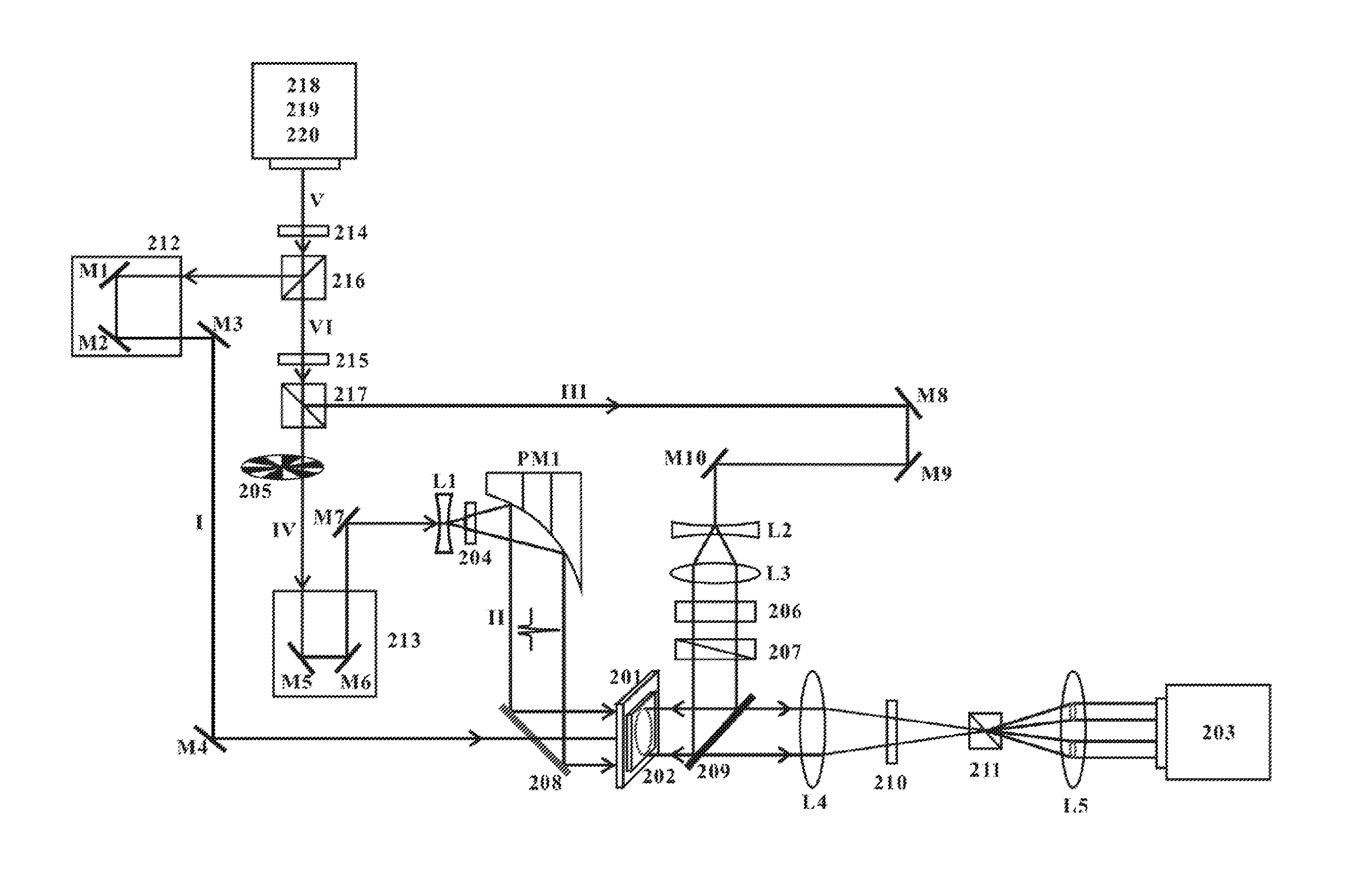
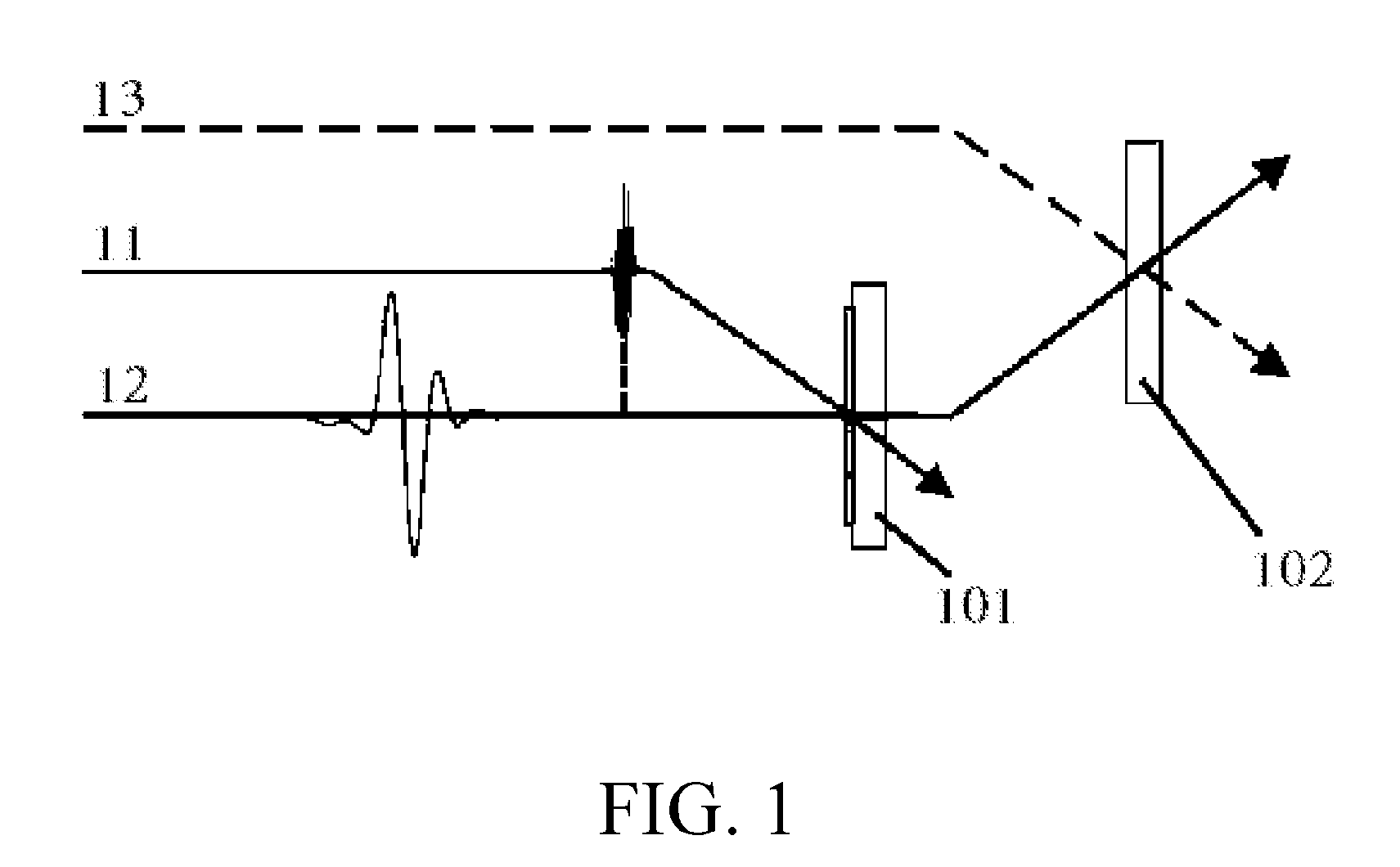
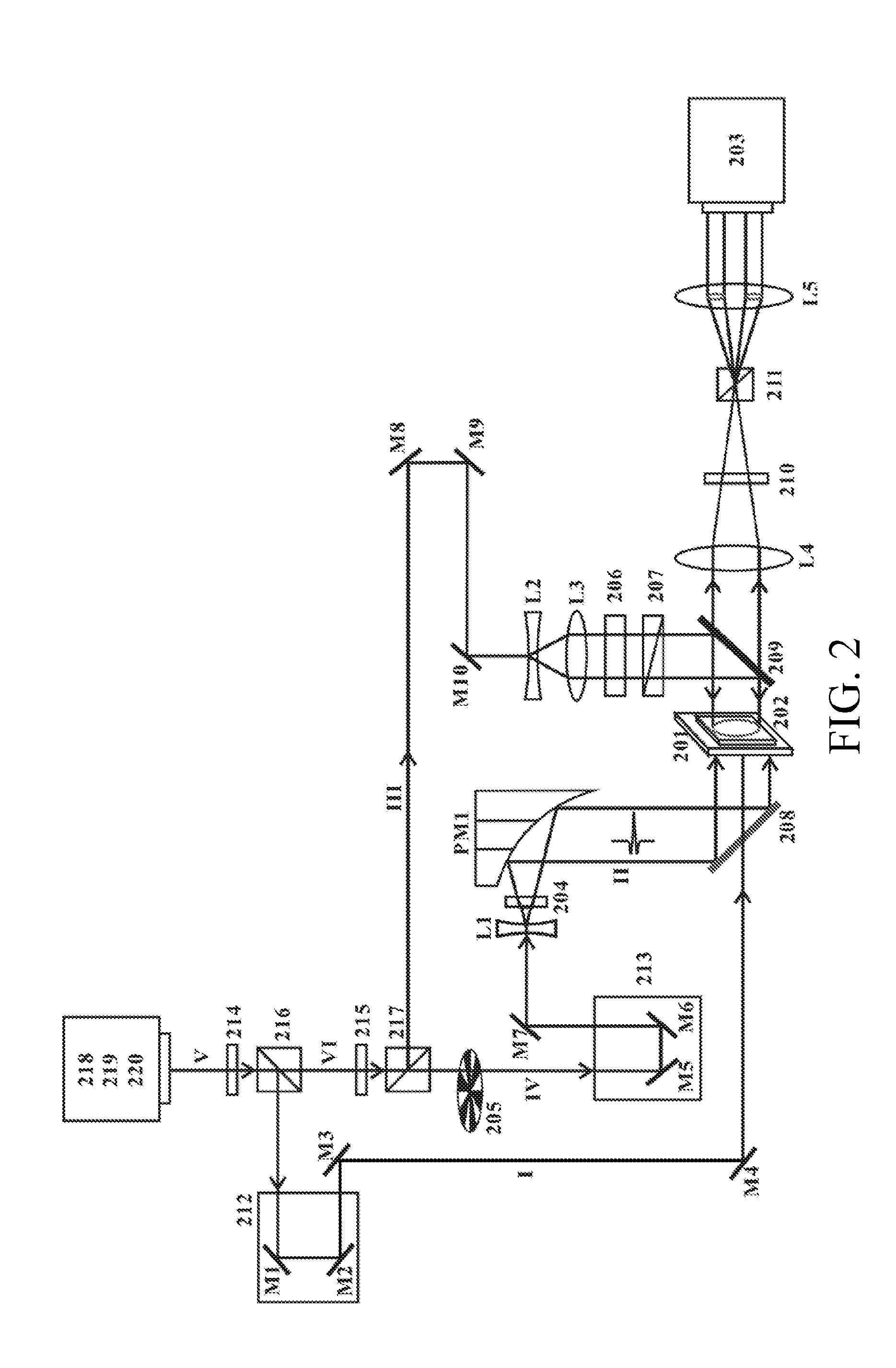
[0082]An imaging system according to the embodiments of the present invention, by introducing a terahertz focal plane imaging technique into a terahertz time-resolved spectrum measurement system, realizes temporal and spatial resolution imaging measurement on light-induced characteristics of the test sample (for example, distribution of semiconductor light-induced carriers); the system is applied to study on temporal and spatial characteristics of semiconductors under optical excitation, and optical digital holography is used for image reconstruction and optimization on original experimental data, thereby achieving comprehensive and accurate observation for temporal and spatial evolution of the semiconductor light-induced carriers.

[0083]FIG. 2 is a schematic view of a terahertz temporal and spatial resolution imaging system according ...


PUM


Abstract

A terahertz temporal and spatial resolution imaging system is provided. The system includes: a sample placing rack; a detection crystal, located on the exit side of the sample placing rack; a pump light generating device, for generating a pump light to irradiate the test sample; a terahertz light generating device, for generating a terahertz light to irradiate the test sample, irradiate the detection crystal after obtaining information about the test sample, and modulate an index ellipsoid of the detection crystal; a detection light generating device, for generating a detection light to irradiate the detection crystal to detect the index ellipsoid of the detection crystal, thereby indirectly obtaining the information about the test sample; and an imaging apparatus, located in an optical path after the detection light passes through the detection crystal, for collecting terahertz images of the test sample.

Description

BACKGROUND OF THE INVENTION[0001]1. Field of the Invention[0002]The present invention relates to the field of optics, and in particular, to a terahertz temporal and spatial resolution imaging system, an imaging method and an application thereof.[0003]2. Related Art[0004]With development of semiconductor manufacturing processes and materials, electronic chips have a higher operation speed, a smaller area, and a lower cost. As phase transition of semiconductors with external excitation is determined by transport characteristics of carriers thereof, the study on the carrier transport phenomena is the foundation of semiconductor device research and development. The terahertz (referred to as THz) pulse technique, as a unique far-infrared measurement means, has demonstrated its significant application potential in the current scientific research and industrial detection. Especially in the study on the semiconductor carrier characteristics, as the terahertz pulse has a low photon energy, a...

Claims


Application Information

Patent Timeline
Patent Type & Authority Applications(United States)
IPC IPC(8): G01J1/42G06T7/00G01J1/04
CPCG01J1/4257G06T7/0004G01J1/0407G01J3/42G01N21/3586
Inventor ZHANG, YANWANG, XINKE
Owner CAPITAL NORMAL UNIVERSITY
Why Eureka
Try Eureka