Semiconductor device

a technology of semiconductors and circuits, applied in the direction of semiconductor devices, basic electric elements, electrical equipment, etc., can solve the problems of reducing the switching speed at turning off, requiring further reducing the on-voltage, etc., and achieve the effect of improving the switching speed

Inactive Publication Date: 2014-07-31
DENSO CORP
View PDF5 Cites 23 Cited by
  • Summary
  • Abstract
  • Description
  • Claims
  • Application Information

AI Technical Summary

Benefits of technology

[0014]When the semiconductor device is turned off, that is, when the turn-off voltage is applied to the gate electrodes in the first gr...

Problems solved by technology

However, recently, it is required to further reduce the on-voltage.
However, in the semiconductor device in the patent document 1, there is a ...

Method used


Image

  • Semiconductor device
  • Semiconductor device
  • Semiconductor device

Examples


first embodiment

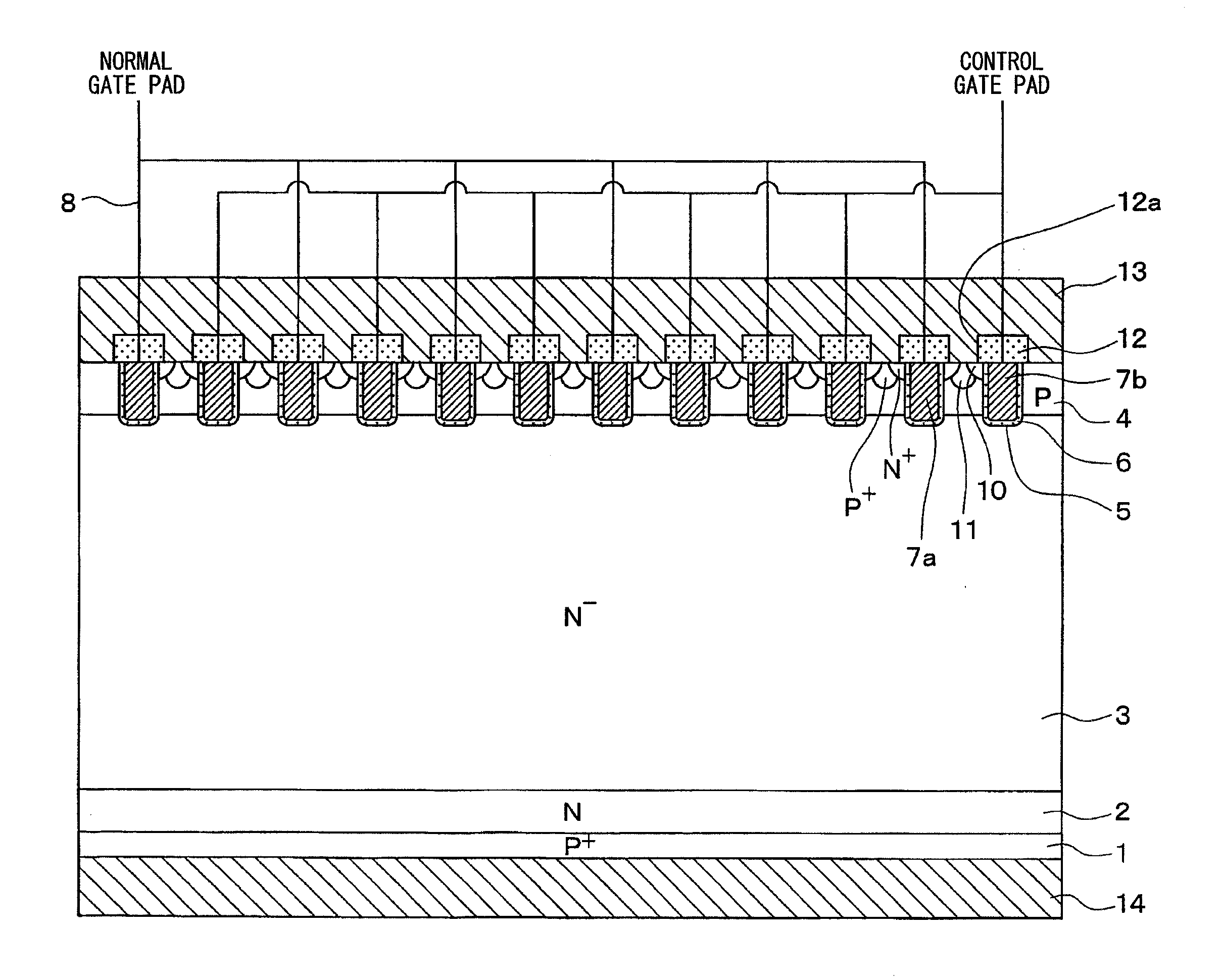
[0024]A semiconductor device according to a first embodiment of the present disclosure will be described with reference to the drawings.

[0025]As illustrated in FIG. 1, an N type field stop layer (hereafter, referred to as an FS layer) 2 is formed above a main surface of a semiconductor substrate that forms a P+ type collector layer 1, and an N− type drift layer 3 is formed above the FS layer 2. Although the FS layer 2 is not always necessary, the FS layer 2 is provided to restrict a spread of a depletion layer, thereby improving performance of a breakdown voltage and a stationary loss. At a surface portion of the N− type drift layer 3, a P type base layer 4 is formed.

[0026]A plurality of trenches 5 penetrates through the P type base layer 4 to reach the N− type drift layer 3. The trenches 5 are formed at predetermined intervals (pitches) and have a stripe structure extending in parallel in a predetermined direction (in FIG. 1, a direction perpendicular to a paper surface). Here, an ...


PUM


Abstract

In a semiconductor device, gate electrodes in a first group are connected with a first gate pad and gate electrodes in a second group are connected with a second gate pad. The gate electrodes in the first group and the gate electrodes in the second group are controllable independently from each other through the first gate pad and the second gate pad. When turning off, after a turn-off voltage with which an inversion layer is not formed is applied to the gate electrodes in the second group, a turn-off voltage with which an inversion layer is not formed is applied to the gate electrodes in the first group.

Description

CROSS REFERENCE TO RELATED APPLICATION [0001]The present disclosure is based on Japanese Patent Application No. 2011-241220 filed on Nov. 2, 2011, the disclosures of which are incorporated herein by reference.TECHNICAL FIELD [0002]The present disclosure relates to a semiconductor device in which an insulated gate bipolar transistor (hereafter, referred to as IGBT) having a trench gate structure is formed.BACKGROUND ART [0003]Conventionally, as one of semiconductor devices for power conversion, a semiconductor device used for an electronic device such as an industrial motor and in which an IGBT is formed has been known. A general semiconductor device in which an IGBT is formed is configured as follows.[0004]Namely, an N− type drift layer is formed above a P+ type semiconductor substrate that forms a collector layer, a P type base layer is formed in a surface portion of the N− type drift layer, and an N+ type emitter layer is formed in a surface portion of the P type base layer. In ad...

Claims


Application Information

Patent Timeline
IPC IPC(8): H01L29/739
CPCH01L29/7397H01L29/4232H01L29/4236H01L29/4238
Inventor SUMITOMO, MASAKIYOFUKATSU, SHIGEMITSU
Owner DENSO CORP
Why Eureka
Try Eureka