Supercharge Your Innovation With Domain-Expert AI Agents!

Three-terminal light emitting device (LED) with built-in electrostatic discharge (ESD) protection device

a technology of protection device and led, which is applied in the direction of semiconductor devices, semiconductor/solid-state device details, electrical apparatus, etc., can solve the problems of esd, adverse effect of led performance, and uneven light generated by leds

Inactive Publication Date: 2014-08-21
SHARP KK
View PDF1 Cites 9 Cited by
  • Summary
  • Abstract
  • Description
  • Claims
  • Application Information

AI Technical Summary

Benefits of technology

The patent describes a method for creating a three-terminal light emitting device chip using a simplified process that eliminates a deep etching step. The chip includes an LED diode and an ESD diode that share an N region. The chip also has three metal pads for electrical connection: a P-pad for the LED diode, a P-pad for the ESD diode, and an N-pad for both diodes. The method involves forming an n-doped semiconductor layer, an active semiconductor layer, and a p-doped semiconductor layer overlying the substrate. A trench is then formed through the p-doped and active semiconductor layers, exposing the n-doped semiconductor layer. An LED P electrode is formed overlying a region of the p-doped semiconductor layer, separated from the active semiconductor layer by the trench. A diode P electrode is formed overlying another region of the p-doped semiconductor layer, shared with the LED, and an N electrode is formed overlying the exposed n-doped semiconductor layer in the trench, shared by both diodes. The technical effect of this patent is to provide a more simplified and efficient method for creating a three-terminal light emitting device chip with ESD protection.

Problems solved by technology

However, the uniformity of light generated by an LED deteriorates as the LED area size increases.
In addition, the heat generated by a large LED is concentrated, and has an adverse effect of LED performance.
Although GaN based LEDs are commercially available, ESD is still a problem due to the fact that the GaN is usually grown on an insulating substrate, such as sapphire or SiC.
When an ESD event comes to contact with the LED pad, a surge voltage can destroy the device instantly.
The reverse biasing of the LED can permanently damage the cell.
The two-way Si Zener diode in FIG. 2 cannot protect the LED from damage due to this effect.
Although the Si diode is cheap comparing to the LED diode, the packaging of the two together can be costly.
The disadvantage of using this approach is that a deep GaN etch is needed to ensure the isolation between the LED and ESD diodes.

Method used


Image

  • Three-terminal light emitting device (LED) with built-in electrostatic discharge (ESD) protection device
  • Three-terminal light emitting device (LED) with built-in electrostatic discharge (ESD) protection device
  • Three-terminal light emitting device (LED) with built-in electrostatic discharge (ESD) protection device

Examples


Embodiment Construction

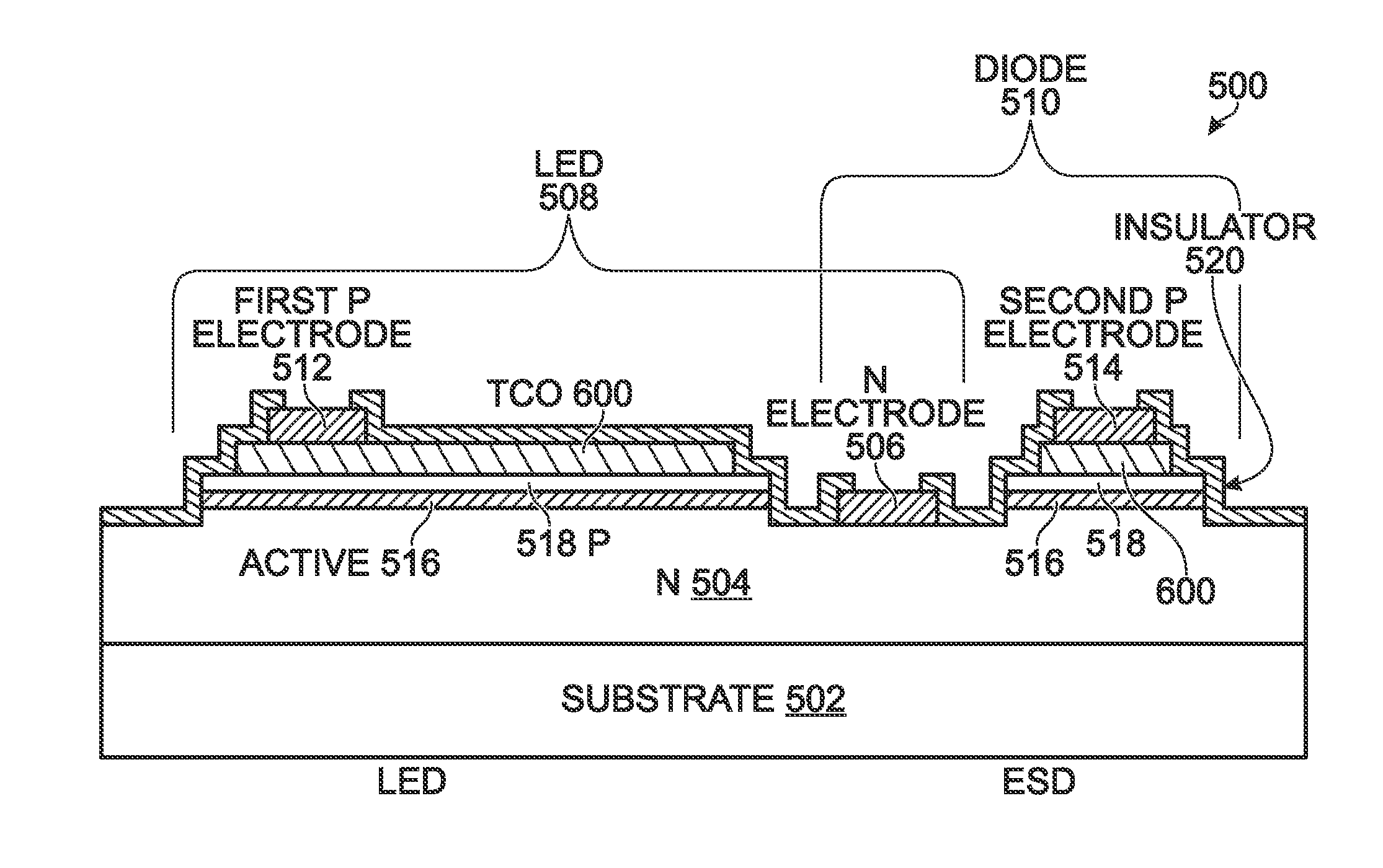
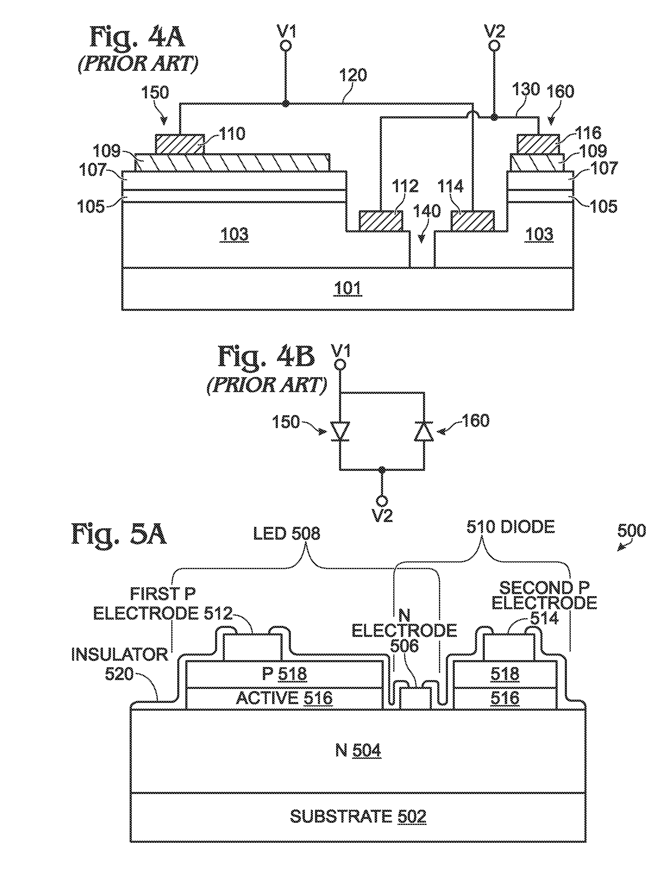
[0022]FIGS. 5A and 5B are, respectively, a partial cross-sectional view of a three-terminal LED chip and a schematic diagram. The LED chip 500 comprises a substrate 502. The substrate 502 may be an insulating material such as quartz, glass, or sapphire, or a semi-insulating material such as silicon (Si), germanium (Ge), Group III-IV compound semiconductors, or Group II-IV compound semiconductors. An n-doped semiconductor layer (N) 504 overlies the substrate 502. An N electrode 506 overlies and is in direct contact with the n-doped semiconductor layer 504. An LED 508 overlies the n-doped semiconductor layer 504, with a first P electrode 512. A diode 510 overlies the n-doped semiconductor layer 504, with a second P electrode 514. The LED 508 and the diode 510 share the N electrode 506.

[0023]In one aspect, the LED 508 comprises an active semiconductor layer 516 overlying and in direct contact with the n-doped semiconductor layer 504. A p-doped semiconductor layer 518 overlies and is in...


PUM


Abstract

A three-terminal light emitting device (LED) chip, associated fabrication method, and LED array are provided. The method forms an n-doped semiconductor layer overlying a substrate, an active semiconductor layer overlying the n-doped semiconductor layer, and a p-doped semiconductor layer overlying the active semiconductor layer. A trench is formed through the p-doped and active semiconductor layers, exposing the n-doped semiconductor layer. In one aspect, the trench is formed at least part way, but not completely, through the n-doped semiconductor layer. Then, an LED P electrode is formed overlying a first region of the p-doped semiconductor layer, a diode P electrode is formed overlying a second region of the p-doped semiconductor layer that is separated from the first region of the p-doped semiconductor layer by the trench, and an N electrode is formed overlying a top surface of the exposed n-doped semiconductor layer in the trench, shared by the LED and diode.

Description

BACKGROUND OF THE INVENTION[0001]1. Field of the Invention[0002]This invention generally relates to a light emitting device (LED) and, more particularly, to a three-terminal LED with built-in electrostatic discharge (ESD) protection for LED array applications.[0003]2. Description of the Related Art[0004]FIG. 1 is a schematic diagram depicting an equivalent circuit for a matrix type light emitting diode (LED), which is also known as a light emitting device (prior art). The luminous efficiency of LEDs has been enhanced drastically in recent years, and it is expected that the LED will replace the conventional incandescent bulb and fluorescent lamp in the future. To generate enough light from an LED to replace an incandescent bulb or fluorescent lamp for general lighting purpose, the area of the LED must be sufficiently large. However, the uniformity of light generated by an LED deteriorates as the LED area size increases. In addition, the heat generated by a large LED is concentrated, ...

Claims


Application Information

Patent Timeline
Patent Type & Authority Applications(United States)
IPC IPC(8): H01L27/15H01L33/42
CPCH01L33/42H01L27/15H01L27/156H01L2924/0002H01L2924/00H01L23/552H01L33/48
Inventor LEE, JONG-JAN
Owner SHARP KK
Features
  • R&D
  • Intellectual Property
  • Life Sciences
  • Materials
  • Tech Scout
  • Unparalleled Data Quality
  • Higher Quality Content
  • 60% Fewer Hallucinations
Learn More