Graphene Ferroelectric Device and Opto-Electronic Control of Graphene Ferroelectric Memory Device

Inactive Publication Date: 2014-08-21
NAT UNIV OF SINGAPORE
View PDF1 Cites 11 Cited by
  • Summary
  • Abstract
  • Description
  • Claims
  • Application Information

AI Technical Summary

Benefits of technology

The invention provides a graphene ferroelectric device that can be used as a non-volatile memory and can be dynamically switched between a transistor and a memory state using a gate bias voltage. The device can also be controlled by photoillumination, and can be used as an optically switchable non-volatile memory. The device is flexible and transparent, and can enter a reversible resistance state in response to photoillumination. The invention also provides a method for controlling the resistance state of a memory device by exposing different elements to different wavelengths of photoillumination.

Problems solved by technology

This method will decrease the device area and the production costs.
However, efforts in this direction are in general constrained by the difficulty of exfoliating and identifying in particular single and bilayer graphene on different substrates.

Method used


Image

  • Graphene Ferroelectric Device and Opto-Electronic Control of Graphene Ferroelectric Memory Device
  • Graphene Ferroelectric Device and Opto-Electronic Control of Graphene Ferroelectric Memory Device
  • Graphene Ferroelectric Device and Opto-Electronic Control of Graphene Ferroelectric Memory Device

Examples


Embodiment Construction

[0025]A description of example embodiments of the invention follows.

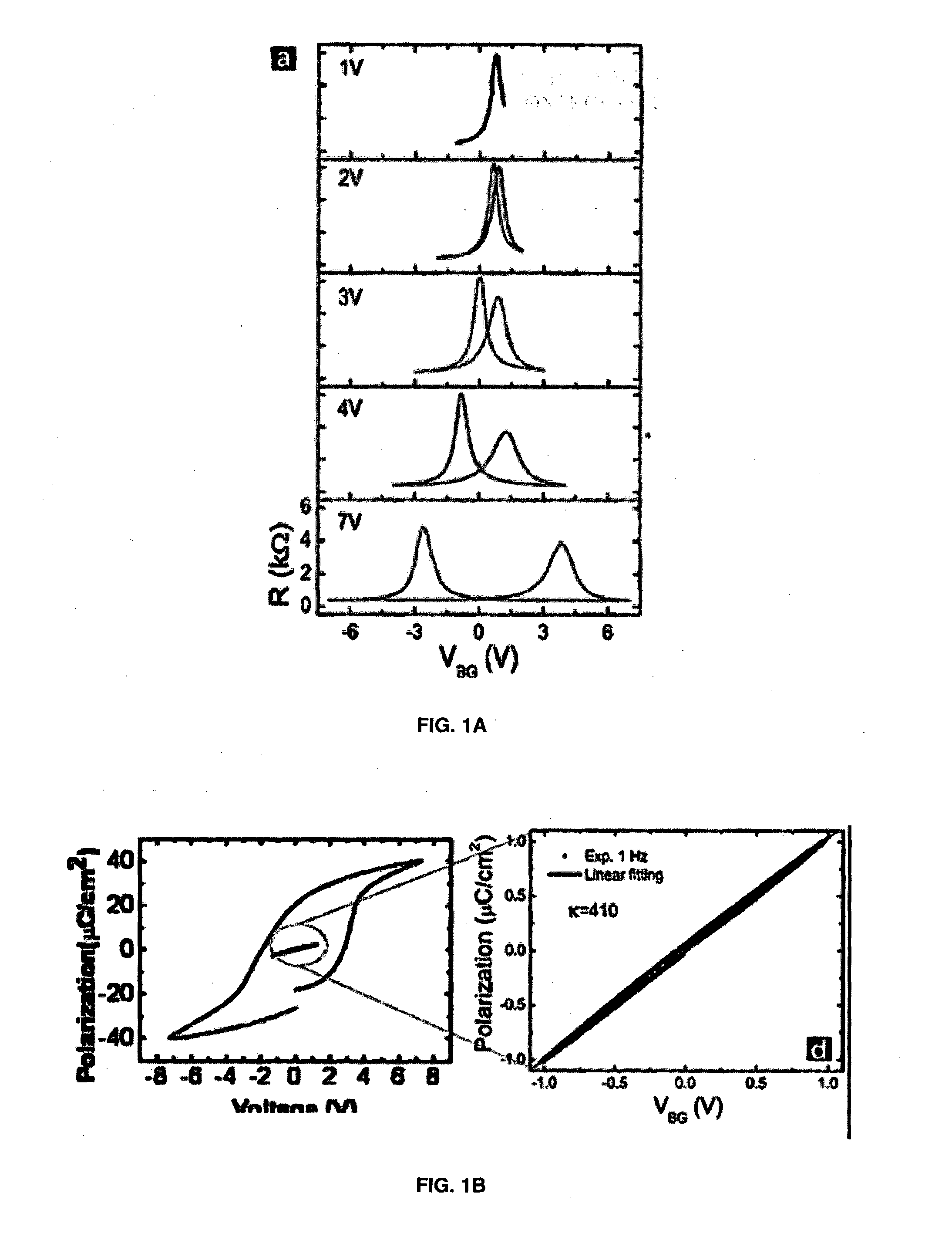
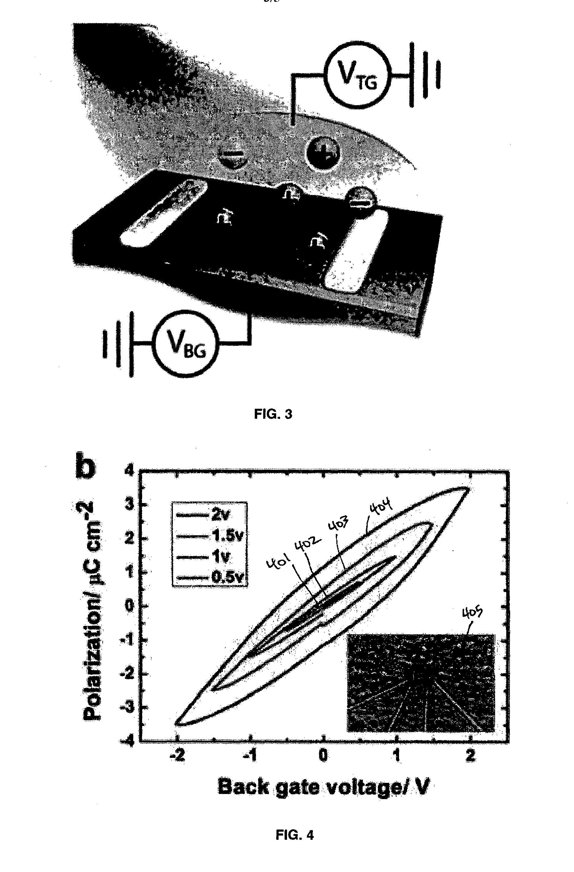
[0026]In accordance with an embodiment of the invention, there is provided a device that can be used as a transistor and a memory simultaneously. This device comprises a graphene field effect transistor (GFET), gated with a special ferroelectric material. A graphene transistor channel has controllable resistance states that are used as binary zeroes and ones. This transistor can be used as a memory, if the ferroelectric is intentionally polarized in a non-volatile manner. A ferroelectric material such as Pb(Zr0.3Ti0.7)O3 (which is a type of lead zirconate titanate, called “PZT” herein) has a linear polarization at low gate voltages. At higher gate voltages it exhibits a large remnant polarization. By taking advantage of this property, a transistor gated with PZT can be used as a normal transistor which operates at low voltages, and if it is gated with higher voltage values it can be used a non-volatile memory. The d...


PUM


Abstract

In accordance with an embodiment of the invention, there is provided a graphene ferroelectric device. The device comprises a graphene transistor channel and a ferroelectric gate of the graphene transistor channel, the ferroelectric gate comprising a linear polarization at a first applied gate voltage less than a threshold voltage, and a hysteretic polarization at a second applied gate voltage greater than the threshold voltage. The device may be configured to undergo optical switching of the graphene transistor channel between a high resistance state and a low resistance state in response to photoillumination of the device.

Description

RELATED APPLICATIONS[0001]This application claims the benefit of U.S. Provisional Application No. 61 / 540,593, filed on Sep. 29, 2011, and claims the benefit of U.S. Provisional Application No. 61 / 569,357, filed on Dec. 12, 2011. The entire teachings of the above applications are incorporated herein by reference.U.S. GOVERNMENT SUPPORT[0002]This invention was made with U.S. government support under Grant No. N62909-10-1-7051 from the U.S. Office of Naval Research Global. The U.S. government has certain rights in the invention.BACKGROUND OF THE INVENTION[0003]Since the first isolation of graphene [1] in 2004, there has been an enormous amount of research done to investigate its properties. Graphene based field effect transistors (FET's) have a very high potential for electronics, especially in terms of high speed, flexibility and transparency. 100 Ghz transistors made of epitaxial graphene have already been shown by IBM [2], which is a speed beyond the theoretical upper limit for tran...

Claims


Application Information

Patent Timeline
IPC IPC(8): G11C11/22H01L43/02
CPCH01L43/02G11C11/223B82Y10/00G11B7/241G11C11/22G11B9/02H01L29/516H01L29/778H01L29/1606G11C13/0002G11C13/04G11C2213/35G11C2213/53B82Y20/00H10N50/80
Inventor OZYILMAZ, BARBAROSKAHYA, ORHANTOH, CHEE TATJAISWAL, MANUSAHA, SURAJIT
Owner NAT UNIV OF SINGAPORE
Why Eureka
Try Eureka