

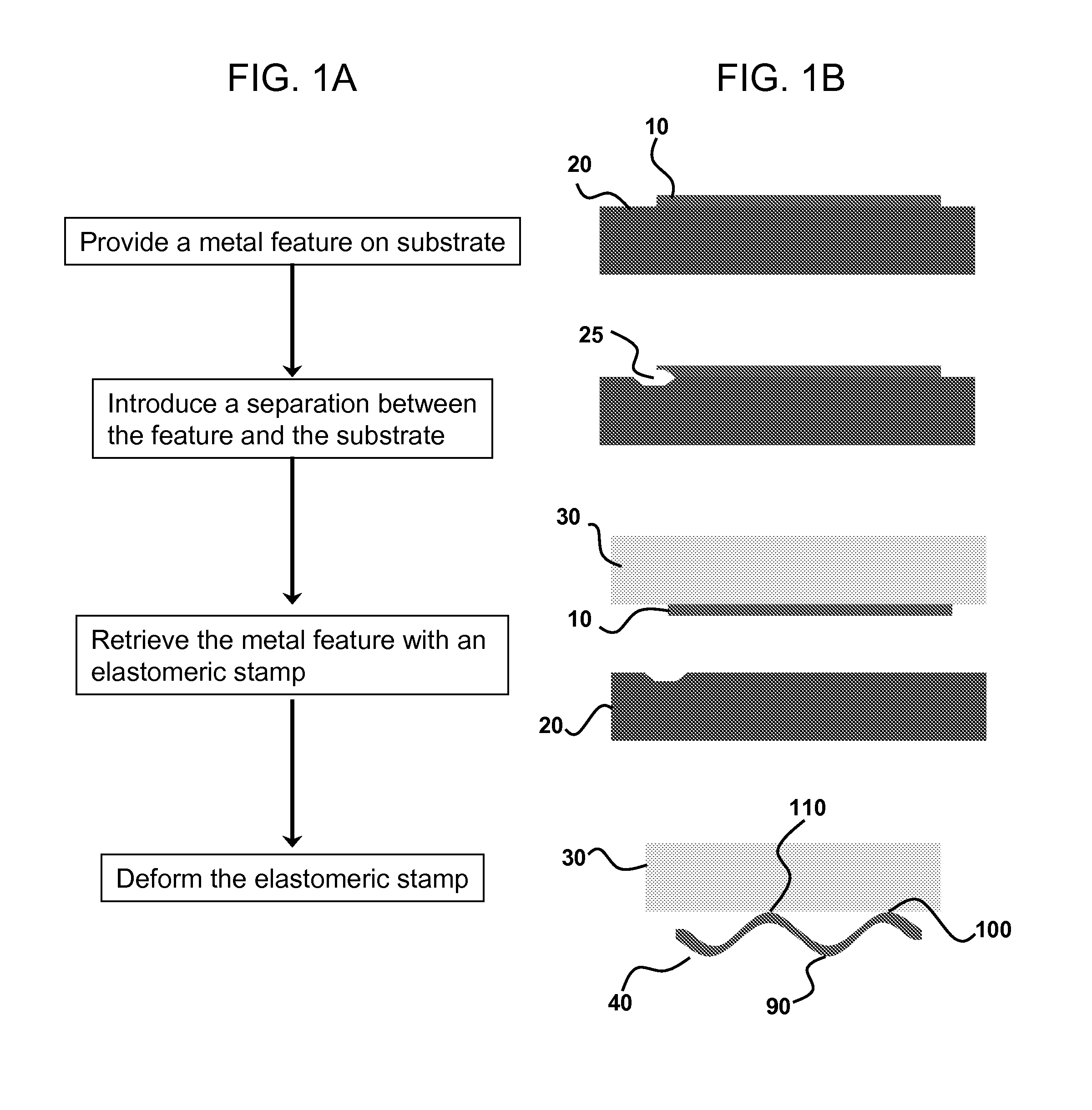
Controlled buckling structures in semiconductor interconnects and nanomembranes for stretchable electronics
a technology of nanomembranes and semiconductors, applied in the direction of thermoelectric devices, semiconductor/solid-state device details, dielectric characteristics, etc., can solve the problems of inability to bind to inorganic semiconductors, and inability to bind to most flexible materials. , to achieve the effect of precise and accurate geometric construction, flexible and bendability, and without adversely affecting performan
- Summary
- Abstract
- Description
- Claims
- Application Information
AI Technical Summary
Benefits of technology
Problems solved by technology
Method used
Image

Examples
example 1
Controlled Buckling Structures in Semiconductor Nanoribbons With Application Examples in Stretchable Electronics
[0183]Control over the compositions, shapes, spatial locations and / or geometrical configurations of semiconductor nanostructures is important for nearly all applications of these materials. Although methods exist for defining the material compositions, diameters, lengths, and positions of nanowires and nanoribbons, there are relatively few approaches for controlling their two- and three-dimensional (2D and 3D) configurations. Provided herein is a mechanical strategy for creating certain classes of 3D shapes in nanoribbons that are otherwise difficult to generate. This example involves the combined use of lithographically patterned surface chemistry to provide spatial control over adhesion sites and elastic deformations of a supporting substrate to induce well-controlled local displacements. Precisely engineered buckling geometries are created in nanoribbons of GaAs and Si ...
example 2
[0208]Our technical approach uses certain ideas embodied in the planar stamp based printing methods previously described. Although these basic techniques provide a promising starting point, many fundamentally new features must be introduced to meet the challenges of the HARDI (Hemispherical Array Detector for Imaging) system, as described in the following.
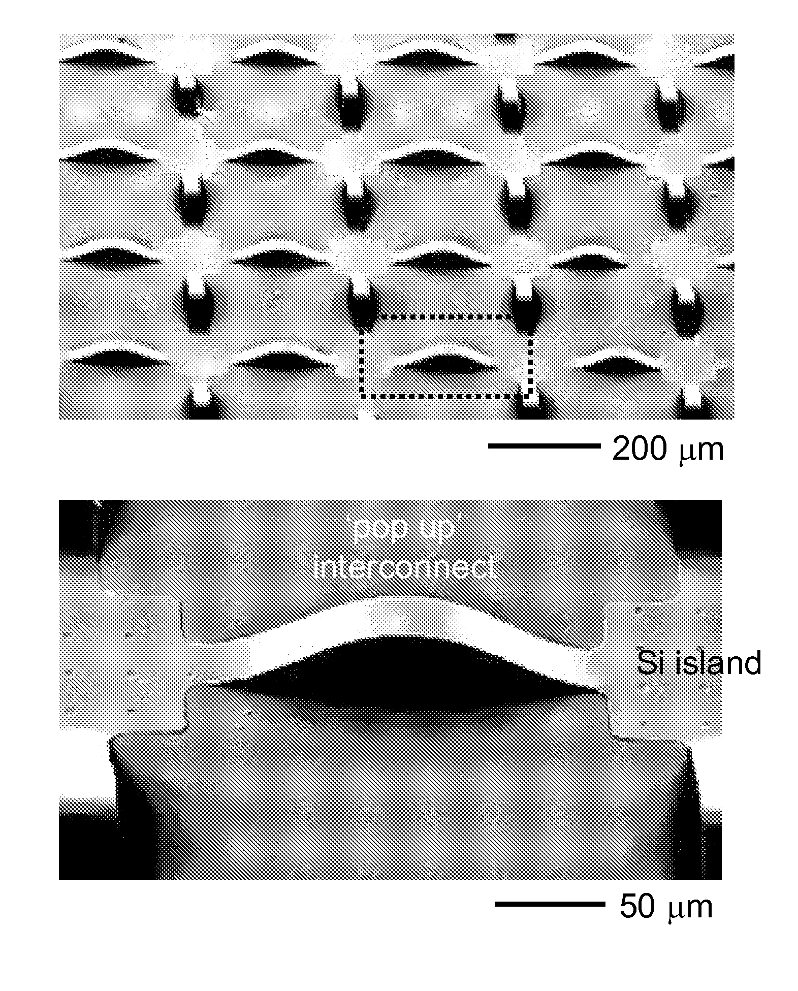
[0209]FIGS. 32 and 33 illustrate a general strategy related to transfer printing to curved surfaces. The first set of steps (FIG. 32) involves the fabrication and manipulation of a thin, spherically curved elastomeric stamp designed to lift off interconnected Si CMOS ‘chiplets’ from the planar surface of a wafer and then to transform the geometry into a hemispherical shape. A stamp for this process is formed by casting and curing a liquid prepolymer to obtain an elastomer such as poly(dimethylsiloxane) (PMDS) against high quality optical elements (i.e. a matched pair of convex and concave lenses) selected with the ...
example 3
Biaxially Stretchable “Wavy” Silicon Nanomembranes
[0220]This example introduces a biaxially stretchable form of single crystalline silicon that consists of two dimensionally buckled, or “wavy”, silicon nanomembranes on elastomeric supports. Fabrication procedures for these structures are described, and various aspects of their geometries and responses to uniaxial and biaxial strains along various directions are presented. Analytical models of the mechanics of these systems provide a framework for quantitatively understanding their behavior. These classes of materials provides a route to high-performance electronics with full, two-dimensional stretchability.
[0221]Electronics that offer mechanically bendability are of interest for applications in information display, X-ray imaging, photovoltaic devices, and other systems. Reversible stretchability is a different and much more technically challenging mechanical characteristic that would enable device possibilities that cannot be realiz...
PUM
| Property | Measurement | Unit |
|---|---|---|
| physical separation distance | aaaaa | aaaaa |
| separation distance | aaaaa | aaaaa |
| thickness | aaaaa | aaaaa |
Abstract
Description
Claims
Application Information