Optical device utilizing optical waveguides and mechanical light-switches

a technology of optical waveguides and mechanical lightswitches, which is applied in the direction of optical waveguide light guides, identification means, instruments, etc., can solve the problems of inefficient power utilization, large size of lcd devices, and high cost, and achieves high efficiency and high cost. , the effect of high cos

Inactive Publication Date: 2003-11-18
LIFE TECH CORP
View PDF12 Cites 186 Cited by
  • Summary
  • Abstract
  • Description
  • Claims
  • Application Information

AI Technical Summary

Problems solved by technology

The CRTs are undesirably large, heavy, and utilize power inefficiently.
These LCD devices are very inefficient.
Moreover, the fabrication processes, especially for active matrix LCDs (AMLCDs), are very complex and expensive.
A high resolution AMLCD requires thousands of addressing lines and millions of transistors on a large substrate, therefore manufacturing is expensive.
Particularly, expensive photolithography has to be used.
As a result, the diagonal of an affordable display is limited.
Other FPD also suffer limitations.
TFEL displays lack efficient blue phosphors and thus have low overall energy efficiency.
PDP technology has been used for commercial production, however manufacturing cost is high and high energy-efficiency displays have yet to be demonstrated.
FED technology potentially is more energy efficient than liquid crystal based displays, however, this potential has not yet been demonstrated.
In addition, manufacturing cost of FEDs currently exceeds that of AMLCDs.
This type of display is presently limited to very large displays such as those used for stadium and outdoor advertisement applications.
The main limitations of matrix LED technology include high cost and impractical manufacture of regular sized displays.
The high cost is due to the necessity of using a large number of LEDs to make the displays.
It is difficult and costly to

Method used


Image

  • Optical device utilizing optical waveguides and mechanical light-switches
  • Optical device utilizing optical waveguides and mechanical light-switches
  • Optical device utilizing optical waveguides and mechanical light-switches

Examples


second embodiment

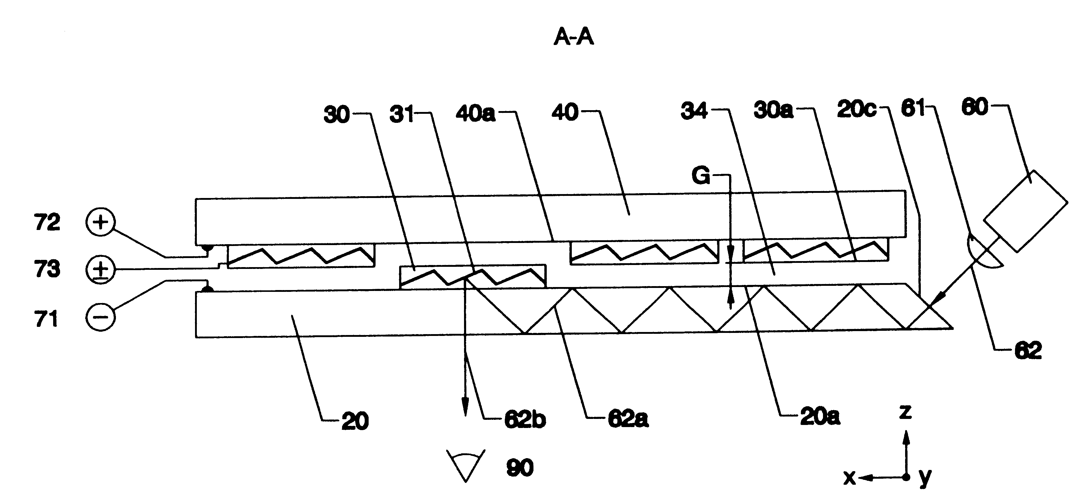
FIG. 5B shows a channel waveguide assembly. In this embodiment, a transparent conductive film 23 is used as the waveguide electrode. The transparent conductive film 23 is preferably made of indium-tin oxide (ITO) while other transparent conductive materials such as doped zinc oxide may also be used. Low optical absorption and high electrical conductivity of the thin film are very important for achieving a high optical efficiency, low power consumption, and fast switching speed in the display device of the present invention. An insulating thin film 24 may be deposited on top of the transparent conductive film 23 to prevent a direct contact between the transparent conductive film 23 and the bottom surface 30a of light switches 30 (FIG. 3). The insulating material can be chosen from a wide selection of dielectrics, such as SiO.sub.2 and phosphor doped SiO.sub.2. The thickness of the transparent conductive film 23 and the insulating thin film 24 is in the range of thousands of Angstroms...

third embodiment

FIG. 5C shows a channel waveguide assembly. Conductor strips 22 are added in cladding 21 regions. The conductor strips 22 are in electrical contact with a transparent conductive film 23. These conductor strips 22 are preferably made of highly conductive metals, such as aluminum, copper, silver, or gold. They are constructed either as single-layer or as multi-layer films. Multilayer structures, if properly constructed, may provide the advantage of improved adhesion to the cladding 21 materials and to the transparent conductive film 23. A transparent conductive film 23 and an insulating thin film 24 are applied on the surface of the waveguide assembly. The construction principles and the materials selected for these thin films are the same as previously described in FIG. 5B. The main advantage of this embodiment is an enhanced conductivity for the waveguide surface electrode with a maximized electrode area. This will result in a lower driving voltage, lower power consumption, and a fa...

example 1

Diffusive Light Switch Device

A working device based on the use of diffusive light switch shown in FIG. 6C was fabricated as follows. Glass plates of 0.5 mm thick were used as planar waveguides for this device. On a glass plate a 1000-.ANG. thick ITO film and a 1000-.ANG. thick SiO.sub.2 film were deposited using a sputtering process. The ITO and the SiO.sub.2 films served as a waveguide electrode and an insulating layer, respectively, as exemplified in FIG. 5B.

Light switches were fabricated by using a procedure similar to that shown in FIGS. 18A through 18C. An ITO / SiO.sub.2 coated glass plate was used as substrate for the light switch fabrication. A 1.2-.mu.m thick aluminum film was deposited on the substrate surface as a sacrificial layer. The deposition was performed in an electron-beam evaporator. A mixture of TiO.sub.2 pigment and a polyimide precursor (Pyralin SP PI-1111 fluorinated polyamic acid from DuPont) was spin-coated on the aluminum surface. The thickness of this layer...


PUM


Abstract

An optical device consists of one or more optical waveguides and mechanical light switches 30. When a light switch 30 is turned on, it extracts light beam 62a from a waveguide core 20 and redirect the light beam 62b into free space, it redirects an incoming light beam 80 from free space and injects the light beam 80a into the waveguide core 20, or it performs both functions at the same time, depending on specific applications. On and off states of a light switch 30 are achieved by pulling the light switch 30 into a close vicinity of the waveguide core 20 and by pushing the light switch 30 away from the waveguide core 20, respectively. An interactive fiat-panel display can be built based on this invention. A plurality of parallel channel waveguides forms a display panel. An array of light beams 62a, injected from an array light source 60, propagates along waveguide cores 20 until reaches a location where a light switch 30 is turned on. At this location, the light switch 30 redirects the light beams towards a viewer. An image is produced when the light switches 30 are turned on sequentially while the light-intensity distribution on the array light source 60 is synchronically updated. The panel display is capable of responding to an input optical signal by detecting an incoming light beam 80 from a light pen 100. An array of photodetectors 81 is used to identify the location of the incoming light beam 80 on the display panel and a computer is used to execute a corresponding action accordingly.

Description

The present invention relates to optical devices, specifically, panel display, with interactive capabilities, which utilizes optical waveguides, mechanical light-switches, and linear-array light sources.DESCRIPTION OF THE RELATED ARTConventional television (TV) sets and computer monitors use cathode ray tubes (CRTs) as display devices. The CRTs are undesirably large, heavy, and utilize power inefficiently. Therefore, there is a genuine need to replace CRTs with thin, light weight and energy efficient flat-panel displays (FPDs).Commercial FPD technologies include liquid crystal displays (LCDs), thin-film electroluminescence (TFEL) displays, plasma display panels (PDPs), field emission displays (FEDs), and light-emitting-diode (LED) matrix displays.Transmissive matrix-LCDs dominate the current FPD market. This type of displays uses a backlight for illumination. These LCD devices are very inefficient. Before reaching a viewer, a light beam must pass through polarizer layers, liquid cry...

Claims


Application Information

Patent Timeline
IPC IPC(8): G02B26/02G02B6/24G02B6/35G02B6/122G09F9/37G09F9/305G09F9/30G02B6/12
CPCG02B6/1221G02B6/241G02B6/3522G09F9/372G02B26/02G09F9/305G02B6/3558G02B2006/12104G02B2006/12145G02B6/357
Inventor ZHOU, XIAOCHUAN
Owner LIFE TECH CORP
Why Eureka
Try Eureka