Disk/pad clean with wafer and wafer edge/bevel clean module for chemical mechanical polishing

a technology of mechanical polishing and clean modules, applied in the direction of cleaning using liquids, cleaning with photosensitive materials, etc., can solve the problems of inability to remove satisfactorily, certain polishing fluids, using cerium oxide,

Active Publication Date: 2014-09-18
APPLIED MATERIALS INC
View PDF3 Cites 9 Cited by
  • Summary
  • Abstract
  • Description
  • Claims
  • Application Information

AI Technical Summary

Benefits of technology

[0074]One advantage of the invention is the relatively small size of the pads 444 and 480 compared to the size of the substrate 100. Conventional systems use large pads positioned on the polishing module to clean smaller substrates, where the substrate is in 100 percent contact with the pad. Large pads are prone to trapping abrasives and particulates which often cause scratches and defects in the substrate. However, the smaller pad of the present invention is significantly less prone to abrasive and particulate trapping, which advantageously results in a cleaner pad and substrates with less scratches and defects. Additionally, the smaller pad of the present invention significantly reduces the cost of consumables, both in the amount of fluid utilized during processing and the cost of replacement pads. Furthermore, the smaller pad of the present invention significantly allows the pad to be easily removed or replaced.

Problems solved by technology

However, certain polishing fluids, for example those using cerium oxide, are particularly difficult to remove and conventionally require processing the substrate in buffing module before being transferred to the cleaning module as conventional cleaning modules have not demonstrated the ability to satisfactorily remove abrasive particles from oxide surfaces that have not been buffed prior to cleaning.

Method used


Image

  • Disk/pad clean with wafer and wafer edge/bevel clean module for chemical mechanical polishing
  • Disk/pad clean with wafer and wafer edge/bevel clean module for chemical mechanical polishing
  • Disk/pad clean with wafer and wafer edge/bevel clean module for chemical mechanical polishing

Examples


Embodiment Construction

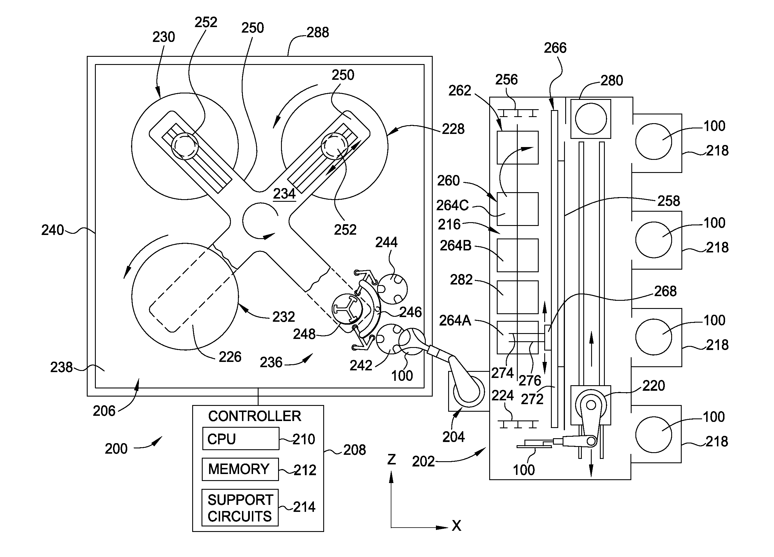
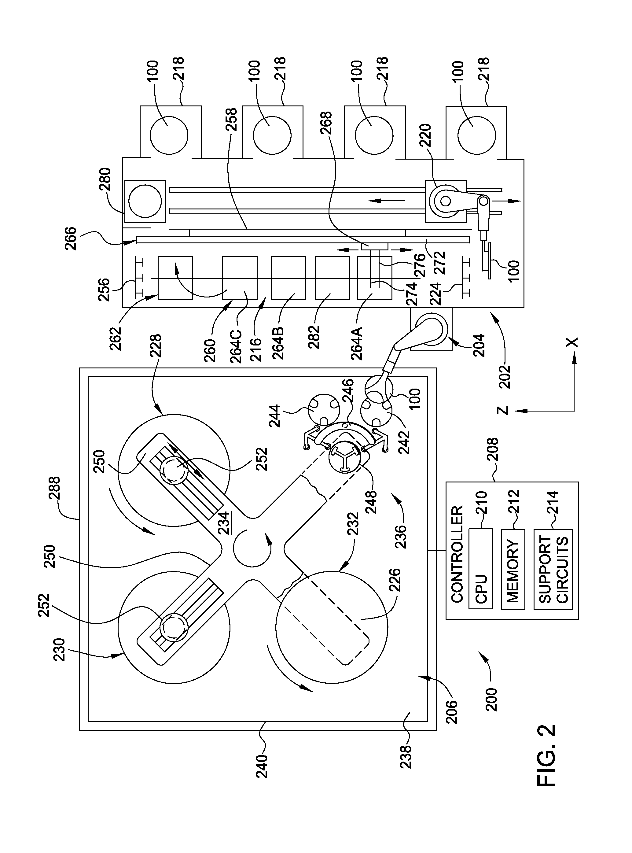
[0032]Implementations of the present invention relate to a method and apparatus for cleaning a substrate after chemical mechanical planarizing (CMP). More specifically implementations of the present invention provide improved methods and apparatus for cleaning and / or polishing the exclusion region and / or edge of a substrate. Abrasive particles (e.g., cerium oxide (CeO)) used in oxide CMP are difficult to remove using traditional PVA brush scrubbing and often require performance of a buffing process on an additional platen on the polishing tool. However even with buffing on the polishing platen particles at the wafer edge (e.g. ≧2 mm) are very difficult to remove.

[0033]Certain implementations described herein provide a clean process where slurry polishing is performed at the exclusion region and / or edge of a wafer after particle cleaning. Certain implementations of the current invention provide an apparatus where a slurry polishing process at the exclusion region and / or edge of a waf...


PUM


Abstract

A method and apparatus for cleaning a substrate after chemical mechanical planarizing (CMP) is provided. The apparatus comprises a housing, a substrate holder rotatable on a first axis and configured to retain a substrate in a substantially vertical orientation, a first pad holder having a pad retaining surface facing the substrate holder in a parallel and space apart relation, the first pad holder rotatable on a second axis rotatable parallel to the first axis, a first actuator operable to move the pad holder relative to the substrate holder to change a distance defined between the first axis and the second axis, and a second pad holder disposed in the housing, the second pad holder having a pad retaining surface facing the substrate holder in a parallel and spaced apart relation, wherein the second pad holder is couple with a rotary arm.

Description

CROSS-REFERENCE TO RELATED APPLICATIONS[0001]This application claims benefit of U.S. Provisional Patent Application Ser. No. 61 / 794,875, filed Mar. 15, 2013, which is herein incorporated by reference in its entirety.BACKGROUND[0002]1. Field[0003]Implementations of the present invention relate to a method and apparatus for cleaning a substrate after chemical mechanical planarizing (CMP).[0004]2. Description of the Related Art[0005]In the process of fabricating modern semiconductor integrated circuits (ICs), it is often necessary to planarize surfaces prior to depositing subsequent layers to ensure accurate formation of photoresist masks and to maintain stack tolerances. One method for planarizing a layer during IC fabrication is chemical mechanical planarizing (CMP). In general, CMP involves the relative movement of the substrate held in a polishing head against a polishing material to remove surface irregularities from the substrate. In a CMP process, the polishing material is wette...

Claims


Application Information

Patent Timeline
Patent Type & Authority Applications(United States)
IPC IPC(8): H01L21/67H01L21/02
CPCH01L21/67051H01L21/02041H01L21/67219H01L21/02065H01L21/02087B08B1/002B08B1/006B08B1/04B08B3/10H01L21/31053H01L21/67046H01L21/67178H01L21/68764
Inventor CHEN, HUIKO, SEN-HOU
Owner APPLIED MATERIALS INC
Why Eureka
Try Eureka