

Semiconductor device and manufacturing method thereof
- Summary
- Abstract
- Description
- Claims
- Application Information
AI Technical Summary
Benefits of technology
Problems solved by technology
Method used
Image

Examples
first example embodiment
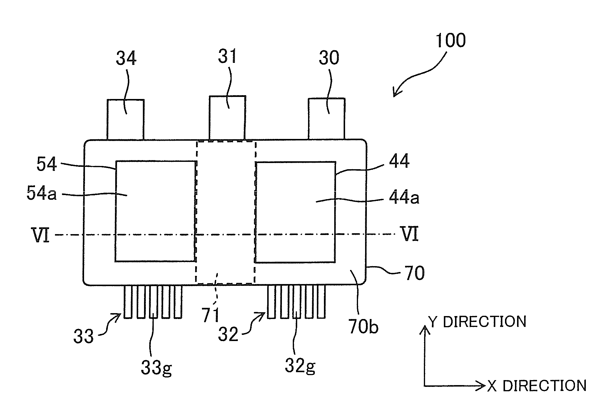
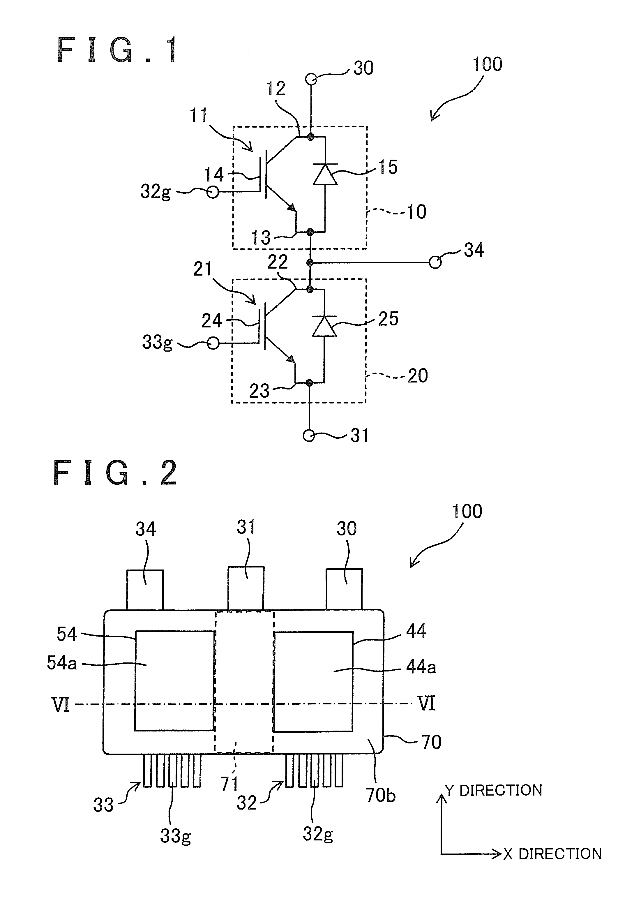
[0039]First, an inverter circuit formed in a semiconductor device 100 will be described.
[0040]As shown in FIG. 1, an inverter circuit provided with a pair of arms, i.e., an upper arm circuit portion 10 and a lower arm circuit portion 20, is formed in the semiconductor device 100.
[0041]The upper arm circuit portion 10 includes an n channel-type IGBT element 11, and a return FWD element 15 that is connected in inverse-parallel to the IGBT element 11. Also, the lower arm circuit portion 20 includes an n channel-type IGBT element 21, and a return FWD element 25 that is connected in inverse-parallel to the IGBT element 21. This IGBT element 11 corresponds to a first semiconductor element described in the claims, and the IGBT element 21 corresponds to a second semiconductor element described in the claims.
[0042]The IGBT element 11 has a collector electrode 12, an emitter electrode 13, and a gate electrode 14. Similarly, the IGBT element 21 has a collector electrode 22, an emitter electrod...
second example embodiment
[0099]In this example embodiment, descriptions of portions common to the semiconductor device 100 described in the example embodiment above will be omitted.
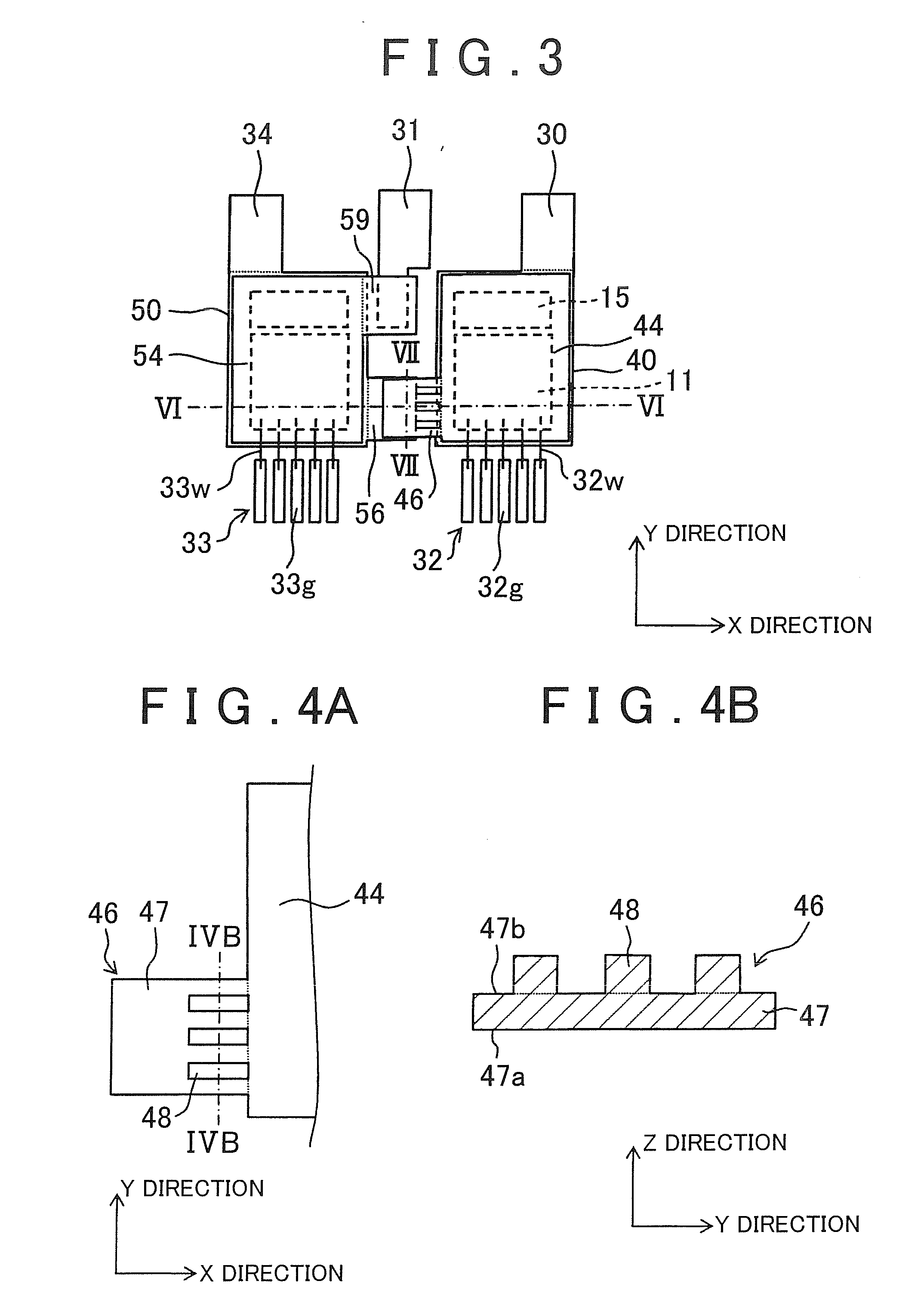
[0100]In this example embodiment, as shown in FIGS. 11 and 12, in addition to the structure described above in the first example embodiment, the first rib 48 is provided extending from the boundary of the first base portion 47 with the second heat sink 44 to the tip end of the first base portion 47 opposite the boundary, in the X direction. This example embodiment is characteristic in that the first rib 48 and the second rib 58 are both provided on the connecting portion where the first connecting surface 47c and the second connecting surface 57c are connected via the solder 60. All other points are the same as in the first example embodiment.
[0101]When the ribs 48 and 58 are provided from the boundaries with the corresponding heat sinks 44 and 50 to the tip ends in this way, the rigidity of the structure described above is able ...
third example embodiment
[0103]In this example embodiment, descriptions of portions common to the semiconductor device 100 described in the example embodiment above will be omitted.
[0104]This example embodiment is characteristic in that, in addition to the structure described above in the second example embodiment, a protruding portion 72 is provided on at least one of the first surface 70a and the second surface 70b of the sealing resin body 70, in the first region 71, as shown in FIGS. 13 and 14.
[0105]In the example shown in FIGS. 13 and 14, the protruding portion 72 is provided on a portion of the first surface 70a in the first region 71 in the X direction. Also, the protruding portion 72 is provided on a portion of the second surface 70b in the first region 71 in the X direction. More specifically, the protruding portion 72 is provided on portions of the first surface 70a and the second surface 70b, which are directly above the connecting portion where the first connecting surface 47c and the second con...
PUM
 Abstract
Description
Claims
Application Information