Electronic component and manufacturing method thereof

a manufacturing method and electronic component technology, applied in the field of coil components, can solve the problems of large variation in height between the conductor pattern and the same conductor layer, increase in dc resistance, insulation failure, etc., and achieve the effects of reducing dc resistance, reducing height variation, and reducing joint strength

Active Publication Date: 2014-09-18
TDK CORPARATION
View PDF2 Cites 28 Cited by
  • Summary
  • Abstract
  • Description
  • Claims
  • Application Information

AI Technical Summary

Benefits of technology

[0018]According to the present invention, the first conductor pattern is formed in such a manner that the first opening region has a concave (or convex) pattern corresponding to a final convex (or concave) shape thereof, and the second conductor pattern is formed on the first conductor pattern, so that the concave (or convex) shape in the lower layer and convex (or concave) shape in the upper layer can be canceled each other to thereby make the top surface of the second conductor pattern as flat as possible. Further, the conductor pattern in the upper layer can be connected to the side surface of the conductor pattern in the lower layer, so that joint strength between the first and second conductor patterns can be enhanced.
[0019]In the present invention, the first conductor layer formation step preferably includes a step of forming a planar coil pattern in addition to the first conductor pattern. When a thickness of the planar coil pattern, such as the spiral conductor, needs to be increased in order to reduce DC resistance, the concave or convex shape of the first conductor pattern formed on the same plane as that on which the planar conductor pattern is formed is further emphasized, with the result that concave or convex shape of the second conductor pattern in a layer formed on the first conductor pattern becomes more noticeable. However, when the first conductor pattern is formed into the shape as described above, the concave shape in the lower layer and convex shape in the upper layer can be canceled each other to reduce a variation in height between the conductor patterns in each conductor layer and thus to make the top surface of the conductor pattern as flat as possible.
[0020]According to the present invention, it is possible to provide an electronic component and a manufacturing method thereof capable of preventing the top surface of the conductor pattern in the topmost layer from bulging or sagging in a lamination process of the conductor pattern and making the same as flat as possible.

Problems solved by technology

However, when a thickness of the coil pattern is excessively small, DC resistance increases.
However, when the coil pattern and another conductor pattern are simultaneously formed under such a plating condition, plating on the another conductor pattern having a comparatively large area grows up excessively, disadvantageously resulting in a large variation in height between the conductor patterns in the same conductor layer.
When the conductor layers each including the conductor patterns varying in height are laminated to achieve a multilayer structure, flatness of a top surface of a conductor pattern formed in a topmost layer is significantly deteriorated due to a cumulative variation in height, which may in turn cause a conductor pattern P2 in the topmost layer to be exposed from the top surface of the insulating layer to lead to an insulation failure.
Further, when the top surface of the conductor pattern serving as a base surface for forming an opening by exposure of an insulating layer covering the conductor patterns bulges or sags, irregular reflection is caused on the top surface to cause defocus in an exposure unit, which degrades pattern processing accuracy.

Method used


Image

  • Electronic component and manufacturing method thereof
  • Electronic component and manufacturing method thereof
  • Electronic component and manufacturing method thereof

Examples


Embodiment Construction

[0034]Preferred embodiments of the present invention will be explained below in detail with reference to the accompanying drawings.

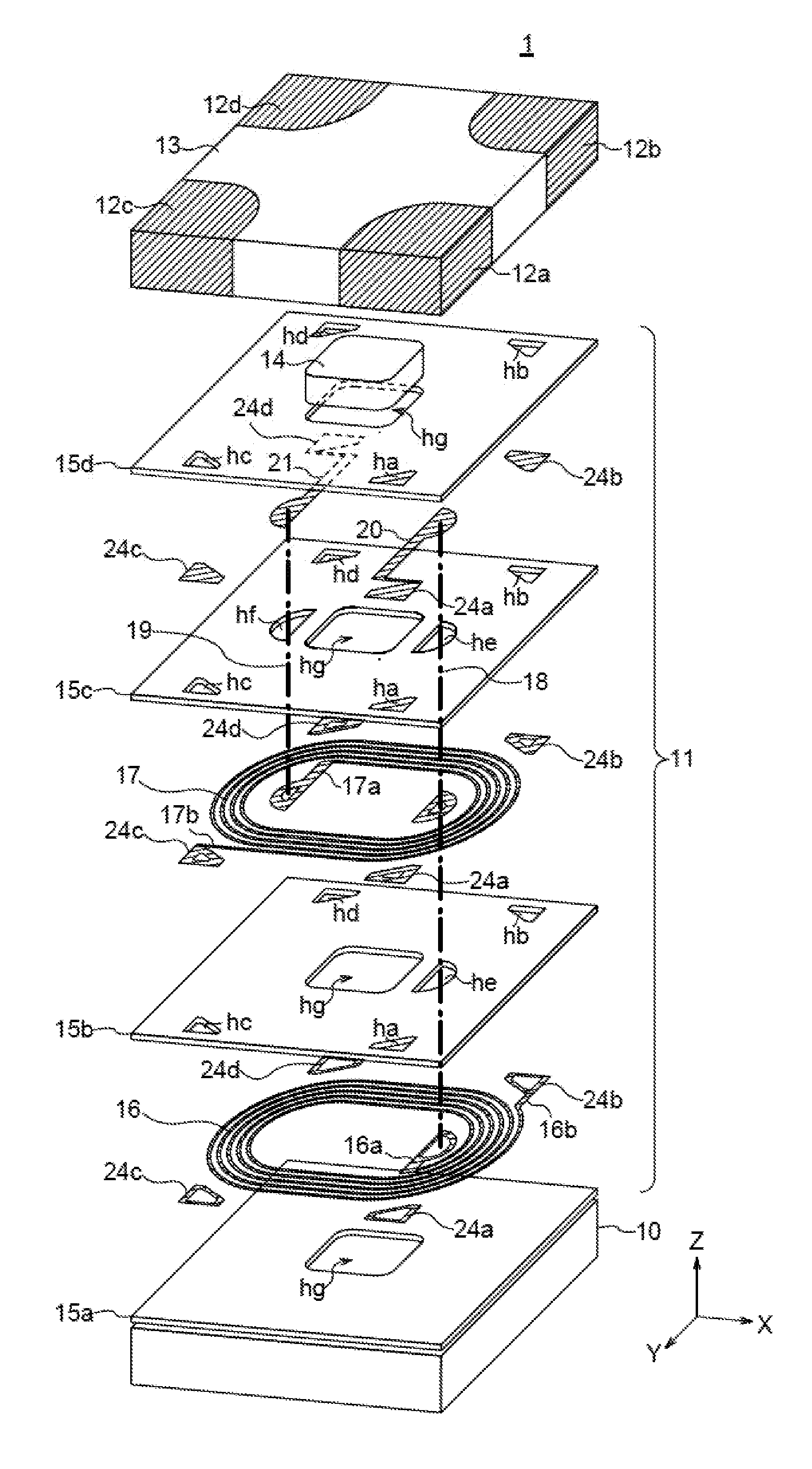
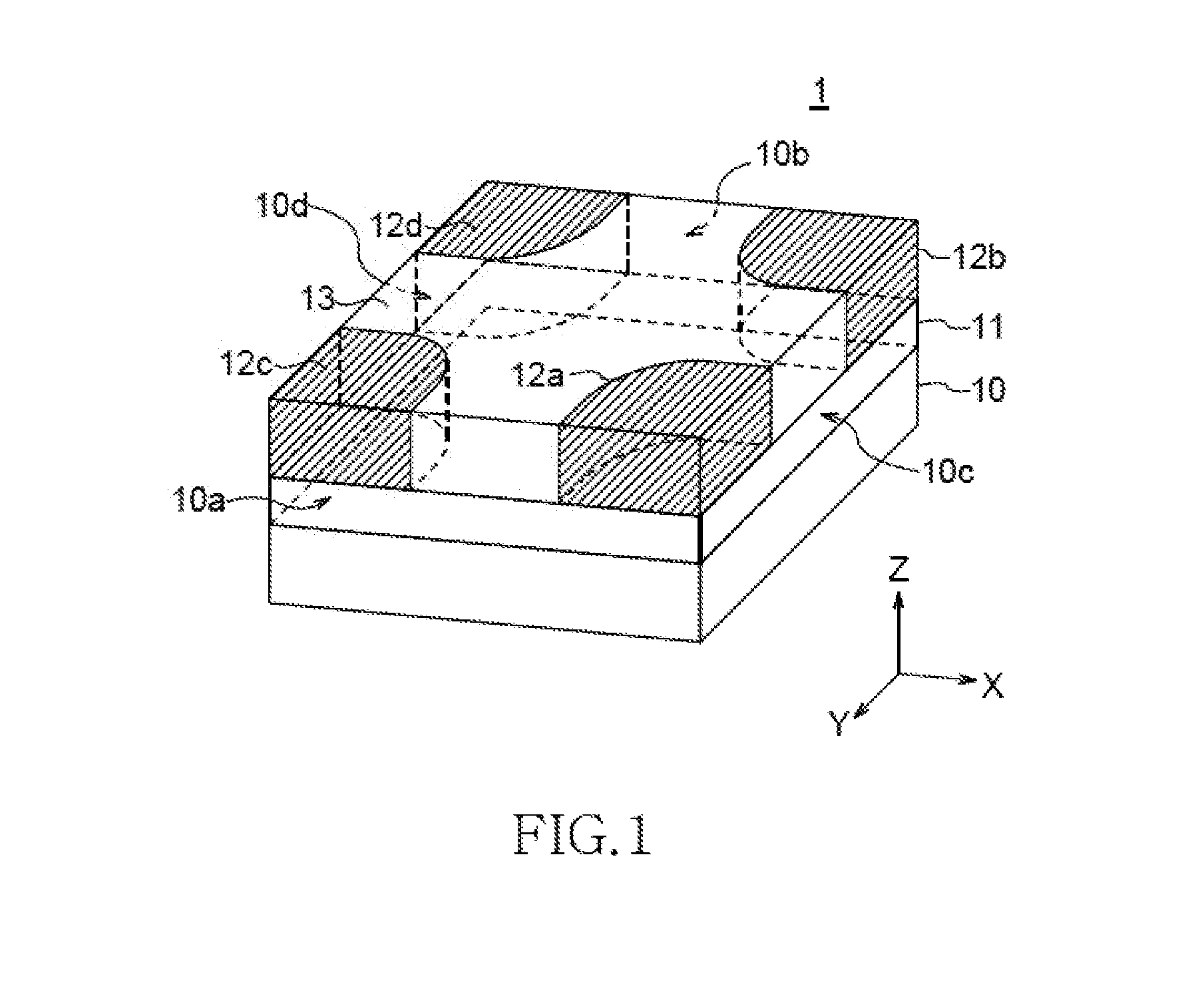
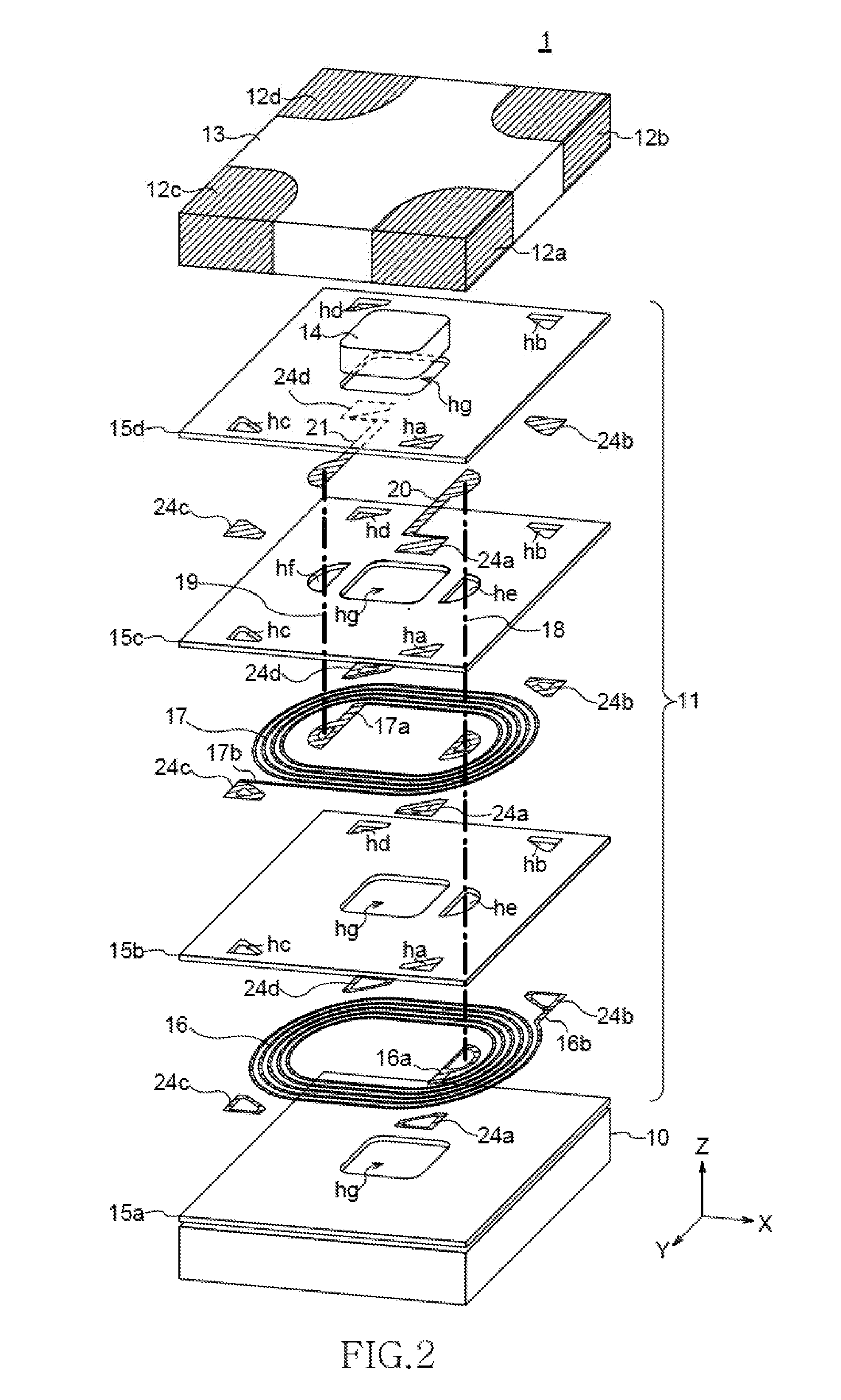
[0035]FIG. 1 is a schematic perspective view showing a structure of a coil component 1 that is an electronic component according to a first embodiment of the present invention.

[0036]As shown in FIG. 1, a coil component 1 according to the present embodiment is a common mode filter and includes a substrate 10, a thin-film coil layer 11 including a common mode filter element provided on one main (top) surface of the substrate 10, first to fourth bump electrodes 12a to 12d provided on one main (top) surface of the thin-film coil layer 11, and a magnetic resin layer 13 provided on the main surface of the thin-film coil layer 11 excluding formation positions of the bump electrodes 12a to 12d.

[0037]The coil component 1 is a surface mount chip component having a substantially rectangular parallelepiped shape. The coil component 1 has two side surfaces 10a, 10b ...


PUM

PropertyMeasurementUnit
thicknessaaaaaaaaaa
thicknessaaaaaaaaaa
aspect ratioaaaaaaaaaa

Abstract

An electronic component includes a first conductor layer including a first conductor pattern P1, a first insulating layer covering the first conductor layer, a first opening h1 passing through the first insulting layer to expose top and side surfaces of the first conductor pattern P1 therethrough, and a second conductor layer formed on the first insulating layer and including a second conductor pattern P2 connected to the first conductor pattern P1 through the first opening h1. A first opening region which is a planar region inside the first opening h1 includes a first region in which the first conductor pattern P1 is formed and a second region in which the first conductor pattern P1 is not formed. The second conductor pattern P2 is embedded in both the first and second regions of the first opening h1.

Description

BACKGROUND OF THE INVENTION[0001]1. Field of the Invention[0002]The present invention relates to an electronic component and a manufacturing method thereof and, more particularly, to a coil component such as a common mode filter and a manufacturing method thereof.[0003]2. Description of Related Art[0004]A common mode filter, which is known as one of electronic components, is widely used as a noise suppression component for a differential transmission line. Recent progress of manufacturing technology allows the common mode filter to be realized as a very small surface mount chip component (see, for example, Japanese Patent Application Laid-open No. 2011-14747), and a coil pattern to be incorporated is significantly reduced in size and space. However, when a thickness of the coil pattern is excessively small, DC resistance increases. Thus, it is desired to increase the thickness of a planar coil pattern as much as possible so as to prevent the increase in the DC resistance.[0005]In th...

Claims


Application Information

Patent Timeline
Patent Type & Authority Applications(United States)
IPC IPC(8): H01F27/28H01F41/04
CPCH01F41/041H01F27/2804H01F17/0013H01F27/29H01F41/042H01F2017/0066H01F2017/0093Y10T29/4902
Inventor WATANABE, FUMIOISHIKAWA, NAOZUMIKAMIYAMA, HIROSHI
Owner TDK CORPARATION
Why Eureka
Try Eureka