Methods and Systems For Connecting Inter-Layer Conductors and Components in 3D Structures, Structural Components, and Structural Electronic, Electromagnetic and Electromechanical Components/Devices

a technology of interlayer conductors and components, applied in the direction of dielectric characteristics, thermoplastic polymer dielectrics, dielectric associations, etc., can solve the problems of low reliability, low performance, and limited application in large-scale adoption

Active Publication Date: 2014-09-18
BOARD OF RGT THE UNIV OF TEXAS SYST
View PDF3 Cites 74 Cited by
  • Summary
  • Abstract
  • Description
  • Claims
  • Application Information

AI Technical Summary

Benefits of technology

[0010]The present invention provides methods and systems for embedding a filament (e.g., wire, mesh, etc.) in a thermoplastic substrate during the fabrication of a 3D structure that can be geometrically complex and intricate, a structural component, or a structure with embedded electronics, sensors and actuators. In addition, the filament can be embedded in multiple layers of the thermoplastic device. The present invention provides electrical interconnects with conductivity and durability comparable to that of traditional printed circuit board (PCB) technology.

Problems solved by technology

Large-scale adoption has been limited due to the low reliability, low performance and high cost of current low temperature cured, conductive ink-based technology.
Advancement of 3D electronics is primarily limited to a small number of researchers across the world, most of whom are pursuing conductive ink technologies.
These devices exhibit some 3D freedom and have seen widespread use in the automotive and personal communications markets; however, they are limited in application in comparison to the current invention since the conductive traces that result from the plating process are restricted to the exterior surfaces of the molded part that are accessible to the etching laser, and therefore cannot exhibit the embedded, multi-layer capability of the current invention.
Moreover, these electroless plating processes provide limited cross-sectional area of the fabricated conductor and consequently limit high current capability.
These low temperature cured inks have weaknesses in both conductivity and in durability [17], which limit the application of AM fabricated 3D structural electronics to simple devices that are not subject to mechanical shock, vibration, large current or power densities, temperature extremes or applications with high reliability requirements.
This gap in mechanical properties between AM-produced parts and injection molded parts extends passed tensile properties to include impact, flexural, compression, creep, and fatigue properties, which collectively limit the application of AM-produced parts to prototypes.

Method used


Image

  • Methods and Systems For Connecting Inter-Layer Conductors and Components in 3D Structures, Structural Components, and Structural Electronic, Electromagnetic and Electromechanical Components/Devices
  • Methods and Systems For Connecting Inter-Layer Conductors and Components in 3D Structures, Structural Components, and Structural Electronic, Electromagnetic and Electromechanical Components/Devices
  • Methods and Systems For Connecting Inter-Layer Conductors and Components in 3D Structures, Structural Components, and Structural Electronic, Electromagnetic and Electromechanical Components/Devices

Examples


Embodiment Construction

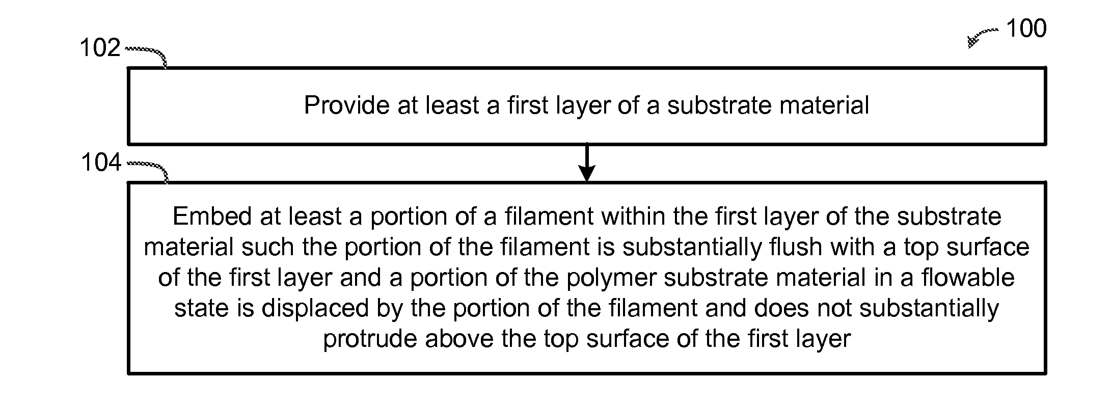
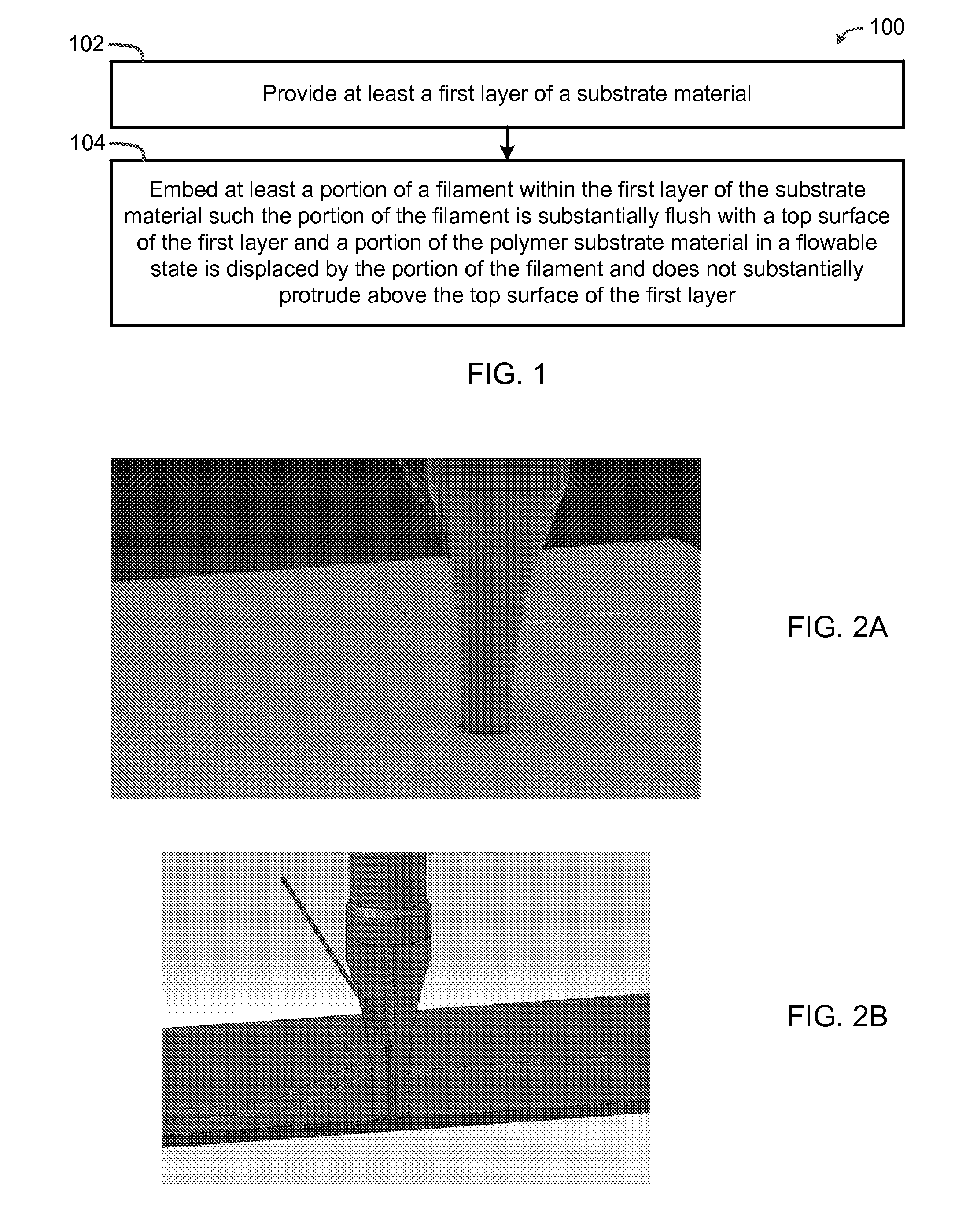
[0044]While the making and using of various embodiments of the present invention are discussed in detail below, it should be appreciated that the present invention provides many applicable inventive concepts that can be embodied in a wide variety of specific contexts. The specific embodiments discussed herein are merely illustrative of specific ways to make and use the invention and do not delimit the scope of the invention.

[0045]To facilitate the understanding of this invention, a number of terms are defined below. Terms defined herein have meanings as commonly understood by a person of ordinary skill in the areas relevant to the present invention. Terms such as “a”, “an,” and “the” are not intended to refer to only a singular entity, but include the general class of which a specific example may be used for illustration. The terminology herein is used to describe specific embodiments of the invention, but their usage does not delimit the invention, except as outlined in the claims....


PUM

PropertyMeasurementUnit
surface areaaaaaaaaaaa
frequencyaaaaaaaaaa

Abstract

The present invention provides systems and methods for creating interlayer mechanical or electrical attachments or connections using filaments within a three-dimensional structure, structural component, or structural electronic, electromagnetic or electromechanical component/device.

Description

CROSS-REFERENCE TO RELATED APPLICATIONS[0001]This application is related to: (1) U.S. patent application Ser. No. 13 / 343,651 filed on Jan. 4, 2012 entitled “Extrusion-Based Additive Manufacturing System for 3D Structural Electronic, Electromagnetic and Electromechanical Components / Devices; and (2) U.S. patent application Ser. No. 13 / 829,723 filed on Mar. 14, 2013 entitled “Methods and Systems for Embedding Filaments in 3D Structures, Structural Components, and Structural Electronic, Electromagnetic and Electromechanical Components / Devices.” These applications are hereby incorporated by reference in their entirety.TECHNICAL FIELD OF THE INVENTION[0002]The present invention relates in general to the manufacture of 3D structures and 3D structural electronic, electromagnetic and electromechanical components and devices, and more particularly to methods and systems for connecting inter-layer conductors and components in three-dimensional structures, structural components, and three dimen...

Claims


Application Information

Patent Timeline
Patent Type & Authority Applications(United States)
IPC IPC(8): H05K3/00H05K1/18
CPCH05K1/183H05K3/0085H05K1/0284H05K2201/0129H05K2201/09036H05K2201/09681H05K2203/0195H05K2203/0285H01L2924/1301H01L24/45H01L24/48H01L24/49H01L24/85H01L2224/45147H01L2224/4813H01L2224/48463H01L2224/4847H01L2224/49175H01L2224/85203H01L2224/85205H01L2224/85214H01L2224/85238H01L2224/85801H01L2924/12042H05K2201/10977H05K2203/049H01L2924/181H01L2924/00014B33Y80/00Y10T29/5193Y10T29/49155H05K3/103H05K3/328H01L2924/00H01L2224/85399H01L2224/05599H01L2224/45144H05K1/0296H05K3/321H05K3/34
Inventor WICKER, RYAN B.MEDINA, FRANCISCOMACDONALD, ERICMUSE, DANNY W.ESPALIN, DAVID
Owner BOARD OF RGT THE UNIV OF TEXAS SYST
Why Eureka
Try Eureka