Scan chain latch design that improves testability of integrated circuits

a technology of integrated circuits and latches, applied in the field of circuit testing, can solve the problems of scan chain adjacency problems, broken/shorted/stuck-at wires, and limited functionality of standard scan chains

Inactive Publication Date: 2014-10-02
IBM CORP
View PDF8 Cites 10 Cited by
  • Summary
  • Abstract
  • Description
  • Claims
  • Application Information

AI Technical Summary

Benefits of technology

[0010]In one embodiment, the two values held in the latches are different values.
[0011]In one embodiment, the scan chain latch circuit has a forward mode of operation and a reverse mode of operation. In the forward mode of operation, a scan-in input is applied to a first of the latches, the data value held in this first latch is applied to the second latch, and this second latch generates a scan-out signal. In the reverse mode of operation, the scan-in signal is applied to the second latch, the data value held on this second latch is applied to the first latch, and the first latch generates the scan-out signal.
[0012]In an embodiment, a scan direction signal is applied to the first and second latches to control whether the latch circuit is in the forward mode of operation or the reverse mode of operation.
[0013]In an embodiment, the first latch includes a first latch multiplexor, and the scan-in signal and an output of the second latch are applied to the first latch multiplexor. The scan direction signal is applied to the first latch multiplexor to control whether the first latch holds the scan-in signal or the output of the second latch.
[0014]In one embodiment, the second latch includes a second latch multiplexor, and the scan-in-reverse input and an output of the first latch are applied to the second latch multiplexor. The scan direction signal is applied to the second latch multiplexor to control whether the second latch holds the scan-in-reverse input or the output of the first latch.
[0015]In an embodiment, the second latch includes a scan-inversion multiplexor, and an inverter sub-circuit for applying an inversion of the output of the first latch to this scan-inversion multiplexor. The output of the second multiplexor is also applied to the scan inversion multiplexor. A scan-inversion signal is applied to a select input of the scan-inversion multiplexor to control whether the output of the second multiplexor or the inversion of the output of the first latch is stored in the second latch.

Problems solved by technology

In this respect, functionality of standard scan chains is quite limited.
Other limitations of standard scan chains include the scan chain adjacency problem, and broken / shorted / stuck-at wires.
The scan chain adjacency problem is the inability to test certain logic state transitions when adjacent latches feed both inputs of the same 2-input AND, NAND, OR, or NOR gate.
A stuck-at fault, which is typically a manufacturing defect, occurs when an input or output of a circuit is stuck at a single logic value.

Method used


Image

  • Scan chain latch design that improves testability of integrated circuits
  • Scan chain latch design that improves testability of integrated circuits
  • Scan chain latch design that improves testability of integrated circuits

Examples


Embodiment Construction

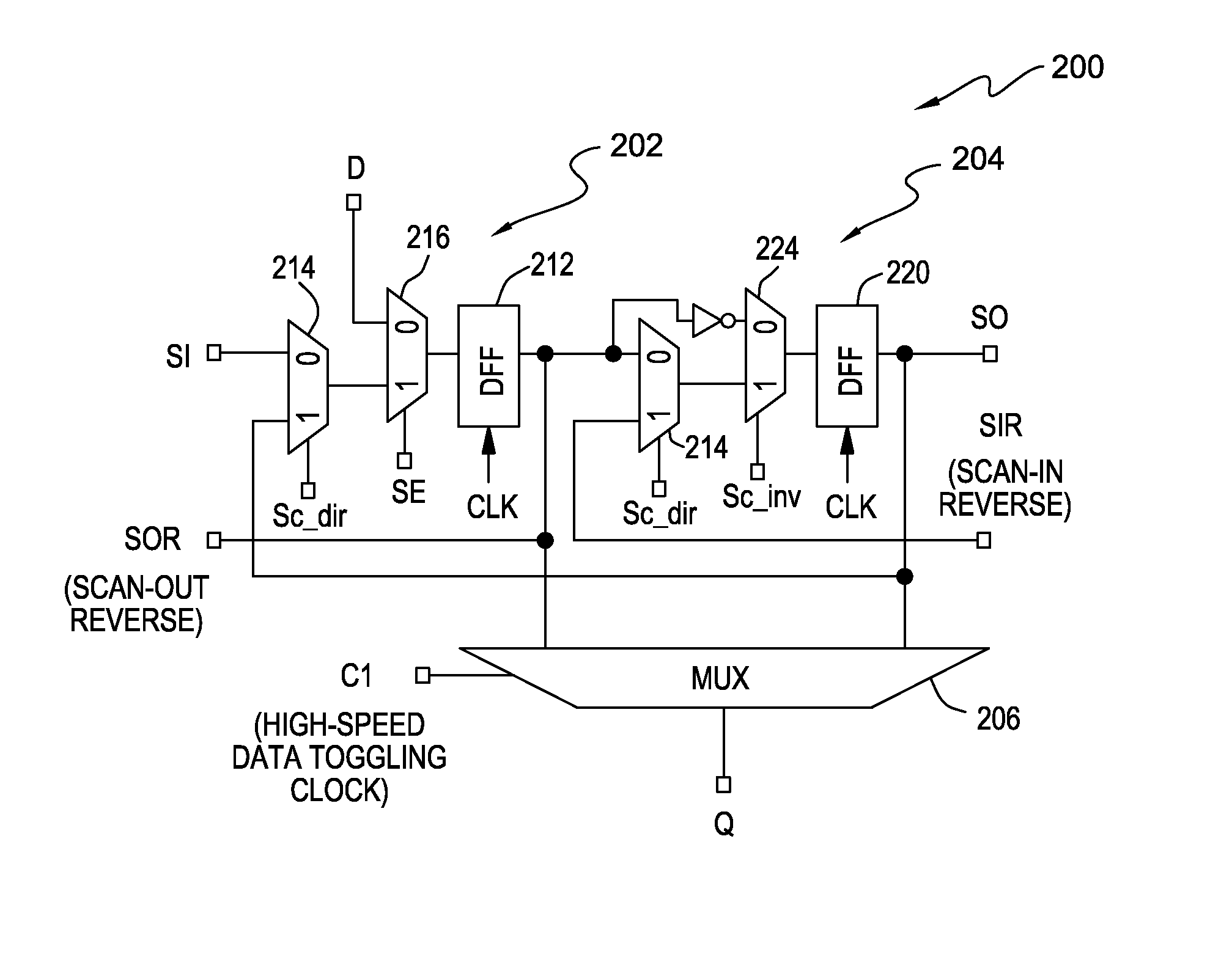
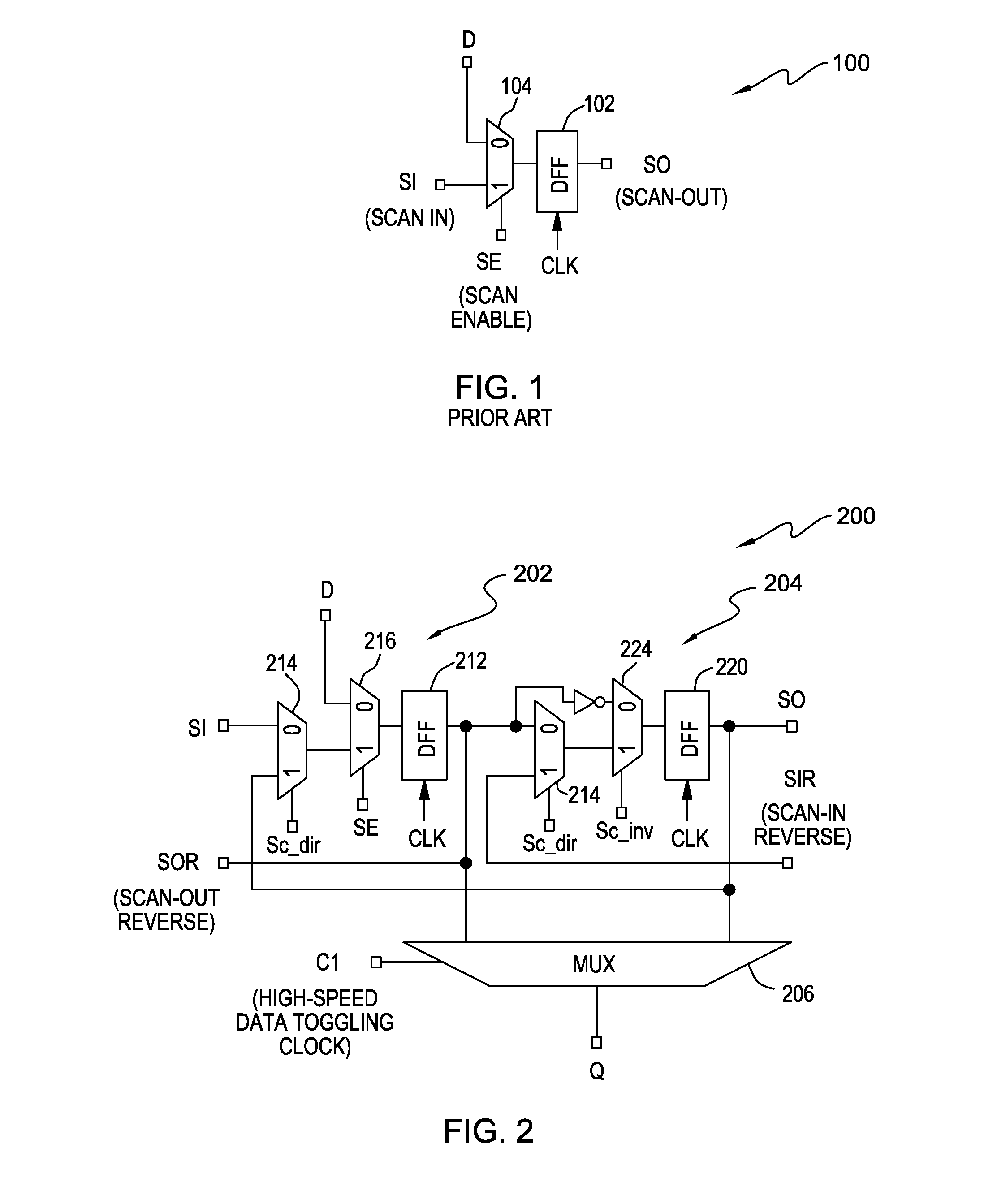
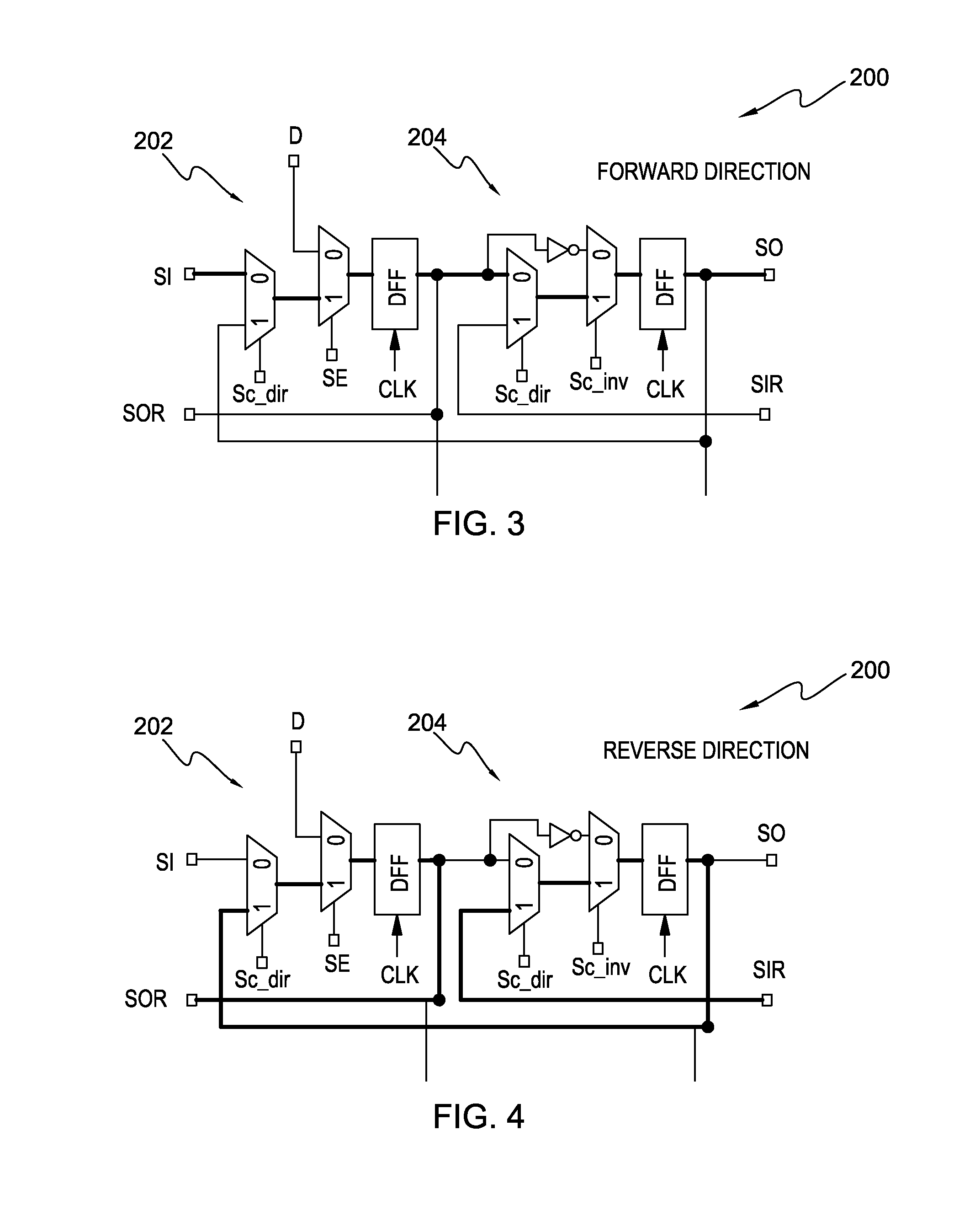
[0025]The present invention relates to scan chains used for integrated circuit diagnostics. Scan chains are widely used in modern IC for rapid test and debug purposes. The recent emergence of emission based test tools imposes additional requirements on scan chains. To extract useful information from emission images, a high degree of control is needed over stimuli applied to a circuit under test. In this respect, functionality of standard scan chains is quite limited. For example, to capture a time resolved emission waveform, the same stimulus may have to be applied thousand or even million times. Using standard scan chain, the entire scan chain would have to be reloaded every time the stimulus is reapplied. This results in unacceptably long acquisition time, because the frequency of stimulus exercising is the frequency of scan chain clock (hundreds of MHz) divided by scan chain length.

[0026]Other limitations of standard scan chains include the scan chain adjacency problem, and broke...


PUM


Abstract

A scan chain latch circuit, a method of operating a latch circuit in a scan chain, and a computer-readable medium having stored thereon a data structure defining a scan chain latch circuit for instantiation on a semiconductor die are disclosed. In an embodiment, the scan chain latch circuit comprises a first latch for holding one data value, a second latch for holding another data value, and a multiplexor. The one data value is applied to a first data input of the multiplexor and the another data value is applied to a second data input of the multiplexor. An alternating clock signal is applied to a select input of the multiplexor to control the output of the multiplexor, wherein the output of the multiplexor toggles between the two data values held in the two latches at a defined frequency.

Description

STATEMENT OF GOVERNMENT INTEREST[0001]This invention was made with Government support under Contract No.: FA8650-11-C-7105 (National Security Agency). The Government has certain rights in this invention.BACKGROUND[0002]The present invention relates generally to circuit testing, and more particularly to scan chains used for circuit diagnostics.[0003]Modern circuit design incorporates methods and hardware that enable circuit testing upon completion of production, often referred to as “design for test” or “design for testability” (DFT). One DFT technique utilizes scan chains. In a scan chain system, certain latches couple together into a hardware connection known as a “scan chain.” The test system inputs a test pattern into the scan chain latches, which the system then uses to test the functionality of the circuit. As such, scan chains allow for increased testability and observability of an integrated circuit design.[0004]Scan chains are widely used in modern IC for rapid test and debu...

Claims


Application Information

Patent Timeline
Patent Type & Authority Applications(United States)
IPC IPC(8): G06F11/26
CPCG06F11/26G01R31/318541G01R31/318519G01R31/318516G01R31/318572G01R31/31727G01R31/3177G01R31/31723
Inventor MALIUK, DZMITRYSTELLARI, FRANCOWEGER, ALAN J.SONG, PEILIN
Owner IBM CORP
Why Eureka
Try Eureka