Flowable silicon-carbon-oxygen layers for semiconductor processing

a technology of silicon carbon-oxygen and flowable silicon, which is applied in the direction of coating, chemical vapor deposition coating, metallic material coating process, etc., can solve the problems of voids or seams, difficult to fill gaps without dielectric materials, and conventional chemical vapor deposition (cvd) techniques often experience an overgrowth of materials, etc., to achieve better etch resistance, improve etch resistance, and increase etch resistance

Active Publication Date: 2014-10-09
APPLIED MATERIALS INC
View PDF3 Cites 38 Cited by
  • Summary
  • Abstract
  • Description
  • Claims
  • Application Information

AI Technical Summary

Benefits of technology

[0009]The final silicon-carbon-oxygen film may exhibit increased etch resistance to both conventional oxide and nitride dielectric etchants. For example, the silicon-carbon-oxygen film may have better etch resistance to a dilute hydrofluoric acid solution (DHF) than a silicon oxide film, and also have better etch resistance to a hot phosphoric acid solution than a silicon nitride film. The increased etch resistance to both conventional oxide and nitride etchants allows these silicon-carbon-oxygen films to remain intact during process routines that expose the substrate to both types of etchants.

Problems solved by technology

As the dimensions continue to get smaller, new challenges arise for seemingly mundane process steps like filling a gap between circuit elements with a dielectric material that acts as electrical insulation.
As the width between the elements continues to shrink, the gap between them often gets taller and narrower, making the gap difficult to fill without the dielectric material getting stuck to create voids and weak seams.
Conventional chemical vapor deposition (CVD) techniques often experience an overgrowth of material at the top of the gap before it has been completely filled.
This can create a void or seam in the gap where the depositing dielectric material has been prematurely cut off by the overgrowth; a problem sometimes referred to as breadloafing.
While the liquid precursor has fewer breadloafing problems, other problems arise when the precursor material is converted to the dielectric material.
The increased porosity left in the final dielectric material can have the same deleterious effects as the voids and weak seams created by conventional CVD techniques.

Method used


Image

  • Flowable silicon-carbon-oxygen layers for semiconductor processing
  • Flowable silicon-carbon-oxygen layers for semiconductor processing
  • Flowable silicon-carbon-oxygen layers for semiconductor processing

Examples


Embodiment Construction

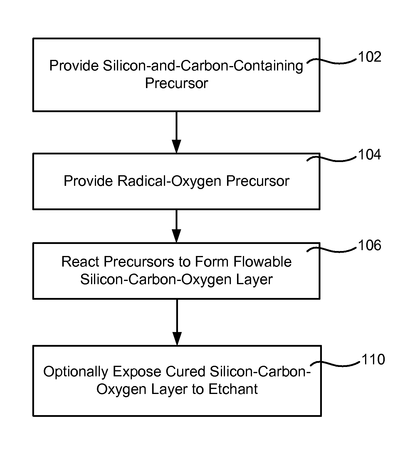
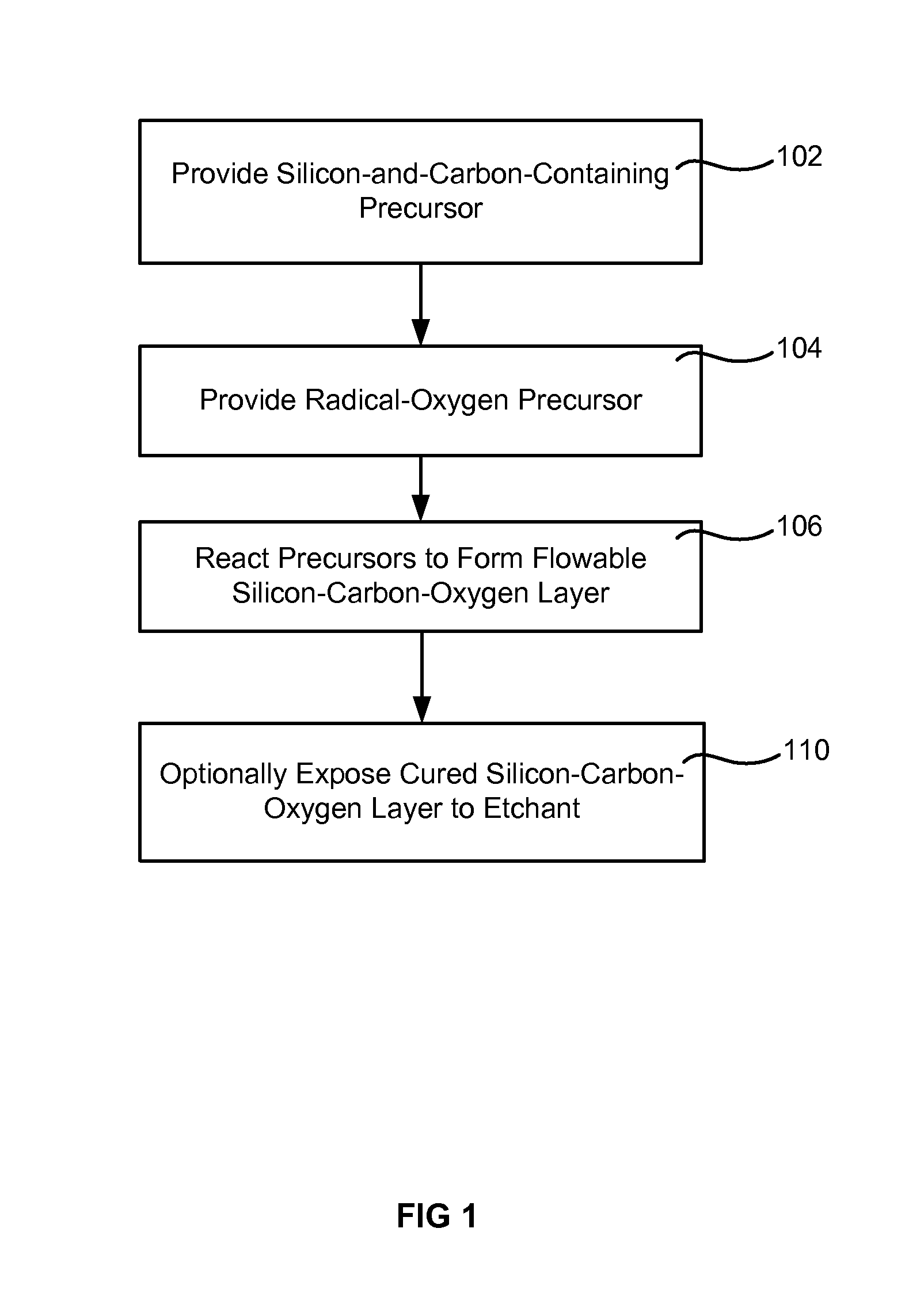
[0017]Methods are described for applying flowable CVD techniques to the formation of flowable silicon-carbon-oxygen containing layers.

[0018]The silicon-and-carbon-containing precursors discussed herein have been found to produce silicon-carbon-oxygen films which have a desirably low wet etch rate despite being flowable during deposition. The silicon-and-carbon-containing precursors contain two distinct silicon atoms separated by one or more intermediate, covalently bonded atoms which may be one or two carbon atoms. For example, the silicon-and-carbon-containing precursor may include a Si—C—Si sequence or a Si—C—C—Si sequence. Larger sequences are also possible (e.g. Si—C—C—C—Si or Si—C—C—C—C—Si) and may include atoms other than carbon between the two distinct silicon atoms. The adjective distinct is used throughout to ensure that the two silicon atoms cannot be construed as a single silicon atom in an atomic ring structure. Each silicon-and-carbon-containing precursor must have at l...


PUM

PropertyMeasurementUnit
temperatureaaaaaaaaaa
sizesaaaaaaaaaa
sizesaaaaaaaaaa

Abstract

Methods are described for forming a dielectric layer on a patterned substrate. The methods may include combining a silicon-and-carbon-containing precursor and a radical oxygen precursor in a plasma free substrate processing region within a chemical vapor deposition chamber. The silicon-and-carbon-containing precursor and the radical oxygen precursor react in to deposit a flowable silicon-carbon-oxygen layer on the patterned substrate. The resulting film possesses a low wet etch rate ratio relative to thermal silicon oxide and other standard dielectrics.

Description

CROSS-REFERENCES TO RELATED APPLICATIONS[0001]This application claims the benefit of U.S. Prov. Pat. App. No. 61 / 808,451 filed Apr. 4, 2013 to Underwood et al., and titled “FLOWABLE SILICON-CARBON-OXYGEN LAYERS FOR SEMICONDUCTOR PROCESSING,” which is hereby incorporated herein in its entirety by reference for all purposes.STATEMENT AS TO RIGHTS TO INVENTIONS MADE UNDER FEDERALLY SPONSORED RESEARCH AND DEVELOPMENT[0002]NOT APPLICABLEREFERENCE TO A “SEQUENCE LISTING,” A TABLE, OR A COMPUTER PROGRAM LISTING APPENDIX SUBMITTED ON A COMPACT DISK[0003]NOT APPLICABLEBACKGROUND OF THE INVENTION[0004]The miniaturization of semiconductor circuit elements has reached a point where feature sizes of 32 nm, 28 nm, and even 22 nm are fabricated on a commercial scale. As the dimensions continue to get smaller, new challenges arise for seemingly mundane process steps like filling a gap between circuit elements with a dielectric material that acts as electrical insulation. As the width between the el...

Claims


Application Information

Patent Timeline
Patent Type & Authority Applications(United States)
IPC IPC(8): H01L21/02
CPCH01L21/02216H01L21/02274H01L21/02126C23C16/401C23C16/452C23C16/45565C23C16/45574H01L21/02208
Inventor UNDERWOOD, BRIAN SAXTONMALLICK, ABHIJIT BASUINGLE, NITIN K.
Owner APPLIED MATERIALS INC
Why Eureka
Try Eureka