Hydroxyl group termination for nucleation of a dielectric metallic oxide

a technology of metallic oxide and hydroxyl group, which is applied in the direction of coating, semiconductor devices, chemical vapor deposition coating, etc., can solve the problems of poor quality differences that are not desirable, and achieve the effect of reducing interfacial defects, facilitating nucleation and deposition of dielectric metal oxides, and reducing differential total thickness

Active Publication Date: 2014-10-16
IBM CORP
View PDF7 Cites 7 Cited by
  • Summary
  • Abstract
  • Description
  • Claims
  • Application Information

AI Technical Summary

Benefits of technology

[0004]A surface of a semiconductor-containing dielectric material is treated with a basic solution in order to provide hydroxyl group termination of the surface. A dielectric metal oxide is subsequently deposited by atomic layer deposition. The hydroxyl group termination provides a uniform surface condition that facilitates nucleation and deposition of the dielectric metal oxide, and reduces interfacial defects between the oxide and the dielectric metal oxide. Further, treatment with the basic solution removes more oxide from a surface of a silicon germanium alloy with a greater atomic concentration of germanium, thereby reducing a differential in the total thickness of the combination of the oxide and the dielectric metal oxide across surfaces with different germanium concentrations.

Problems solved by technology

Poor nucleation results in poor quality of dielectric metal oxides.
Such differences are not desirable because some type of devices incorporate an unnecessarily thick dielectric material layer.

Method used


Image

  • Hydroxyl group termination for nucleation of a dielectric metallic oxide
  • Hydroxyl group termination for nucleation of a dielectric metallic oxide
  • Hydroxyl group termination for nucleation of a dielectric metallic oxide

Examples


Embodiment Construction

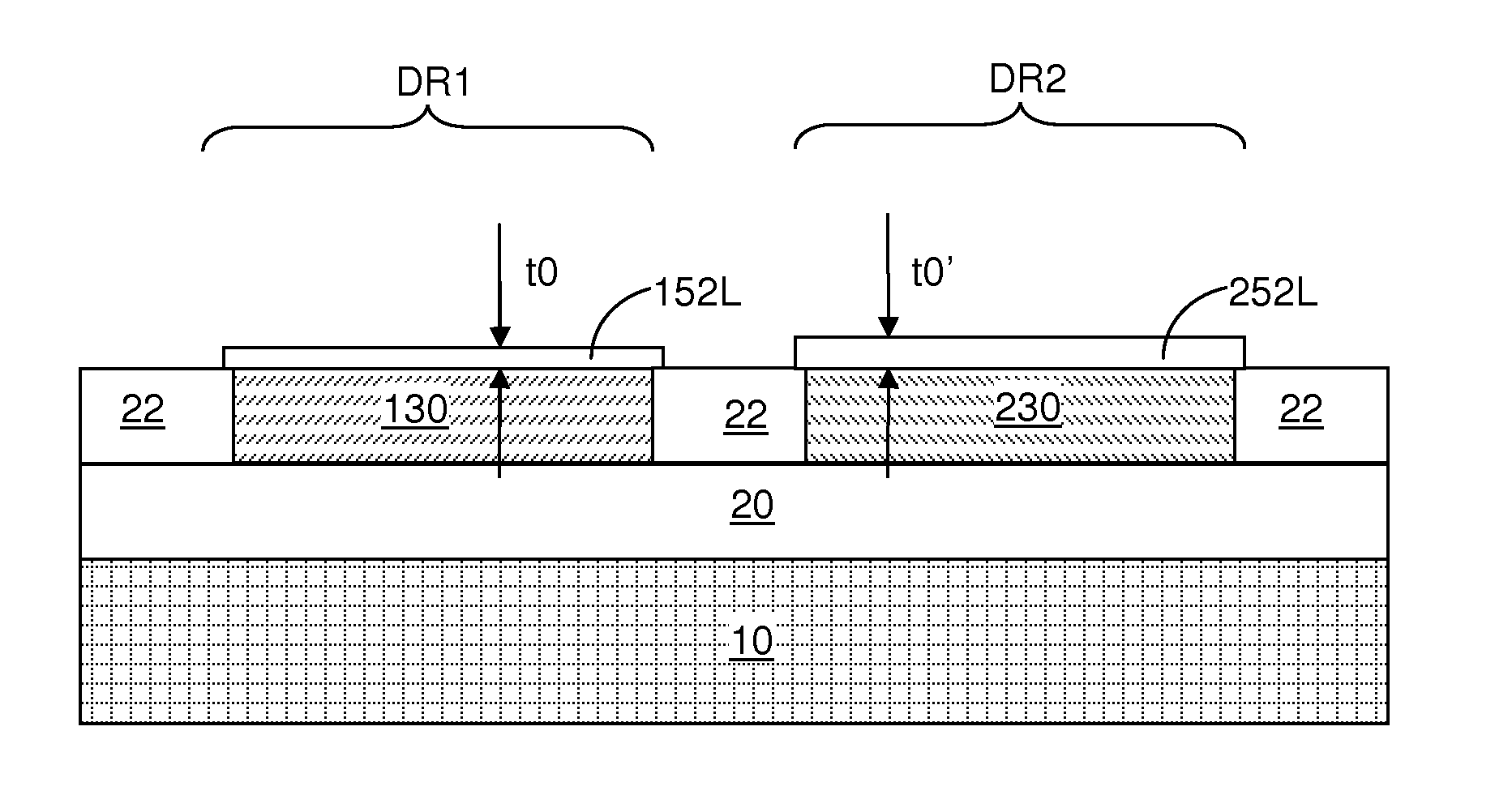
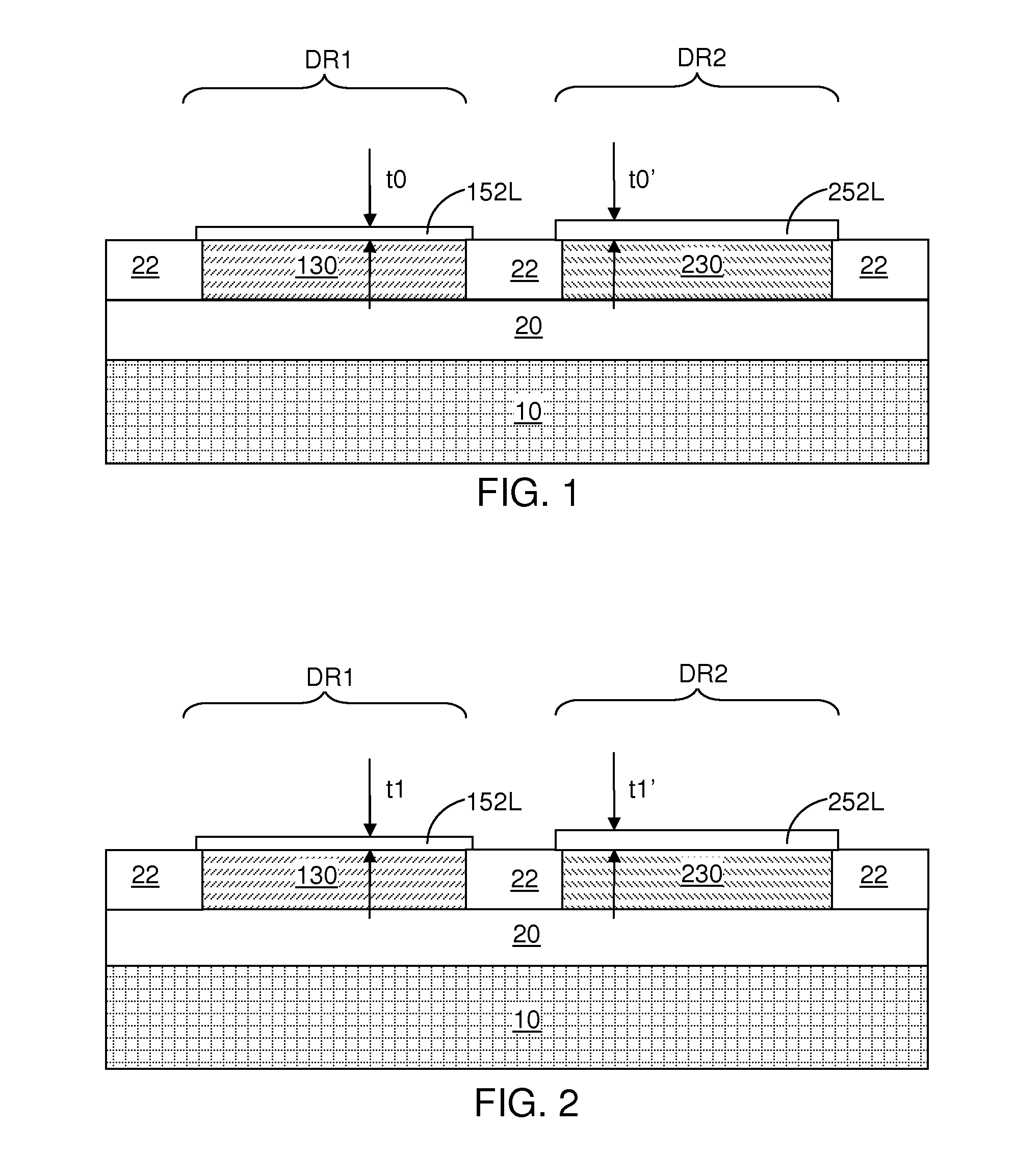
[0017]As stated above, the present disclosure relates to a method of surface treatment of a semiconductor-containing dielectric material for subsequent deposition of a dielectric metal oxide. Aspects of the present disclosure are now described in detail with accompanying figures. It is noted that like reference numerals refer to like elements across different embodiments. The drawings are not necessarily drawn to scale. Ordinals are used merely to distinguish among similar elements, and different ordinals may be employed across the specification and the claims of the instant application.

[0018]Referring to FIG. 1, an exemplary semiconductor structure according to an embodiment of the present disclosure includes a semiconductor substrate, which can be a semiconductor-on-insulator (SOI) substrate or a bulk substrate. The SOI substrate includes a vertical stack, from bottom to top, of a handle substrate 10, a buried insulator layer 20, and a top semiconductor layer. If the semiconductor...


PUM

PropertyMeasurementUnit
thicknessaaaaaaaaaa
thicknessaaaaaaaaaa
thicknessesaaaaaaaaaa

Abstract

A surface of a semiconductor-containing dielectric material / oxynitride / nitride is treated with a basic solution in order to provide hydroxyl group termination of the surface. A dielectric metal oxide is subsequently deposited by atomic layer deposition. The hydroxyl group termination provides a uniform surface condition that facilitates nucleation and deposition of the dielectric metal oxide, and reduces interfacial defects between the oxide and the dielectric metal oxide. Further, treatment with the basic solution removes more oxide from a surface of a silicon germanium alloy with a greater atomic concentration of germanium, thereby reducing a differential in the total thickness of the combination of the oxide and the dielectric metal oxide across surfaces with different germanium concentrations.

Description

BACKGROUND[0001]The present disclosure relates to a method of forming a semiconductor structure, and particularly to a method of surface treatment of a semiconductor-containing dielectric material for subsequent deposition of a dielectric metal oxide.[0002]Nucleation of dielectric metal oxides, such as hafnium oxide, deposited by atomic layer deposition (ALD) is known to be affected by the surface conditions. The thickness and quality of dielectric metal oxides formed by ALD varies according to the surface conditions of an interfacial dielectric material, which is a semiconductor-containing dielectric material such as silicon oxide / oxynitride / nitride or a silicon-germanium oxide / oxynitride / nitride. Poor nucleation results in poor quality of dielectric metal oxides.[0003]In addition, the thickness of an interfacial dielectric material increases with the atomic concentration of germanium in a silicon-germanium alloy material on which the interfacial dielectric material is formed by ch...

Claims


Application Information

Patent Timeline
Patent Type & Authority Applications(United States)
IPC IPC(8): H01L21/02
CPCH01L21/02307H01L21/02172H01L21/0223H01L21/02227H01L21/022H01L21/02301C23C16/0227C23C16/403C23C16/405C23C16/407C23C16/45525H01L21/0214H01L21/02164H01L21/02178H01L21/02181H01L21/02186H01L21/02189H01L21/02192H01L21/02236H01L21/02238H01L21/02247H01L21/02249H01L21/0228H01L21/02312H01L21/28194H01L21/762H01L29/16H01L29/161H01L29/513H01L29/517H01L29/518
Inventor ANDO, TAKASHICHUDZIK, MICHAEL P.DAI, MINFRANK, MARTIN M.HILSCHER, DAVID F.KRISHNAN, RISHIKESHLINDER, BARRY P.ORTOLLAND, CLAUDESHEPARD, JR., JOSEPH F.
Owner IBM CORP
Why Eureka
Try Eureka