Transition metal chalcogenide compound horizontal homogeneous junction solar cell and preparation method thereof

A transition metal chalcogenide, solar cell technology, applied in circuits, electrical components, photovoltaic power generation, etc., can solve the problems of mismatch of work function between electrodes and thin films, inability to form good ohmic contact, stress and metal diffusion, etc. The effect of improving the lighting characteristics, reducing the interface defects and increasing the area

Inactive Publication Date: 2019-04-12
HUAZHONG UNIV OF SCI & TECH
View PDF7 Cites 7 Cited by
  • Summary
  • Abstract
  • Description
  • Claims
  • Application Information

AI Technical Summary

Problems solved by technology

[0004] The invention solves the problems of high lattice mismatch rate and large interface defects in the process of forming the p-n junction of the transition metal chalcogenide film semiconductor material in the prior art, and the damage, stress and metal damage caused by the electrode to the film during the preparation process. Diffusion, and the technical problem of mismatching the work function of the electrode and the film to form a good ohmic contact

Method used


Image

  • Transition metal chalcogenide compound horizontal homogeneous junction solar cell and preparation method thereof
  • Transition metal chalcogenide compound horizontal homogeneous junction solar cell and preparation method thereof
  • Transition metal chalcogenide compound horizontal homogeneous junction solar cell and preparation method thereof

Examples


preparation example Construction

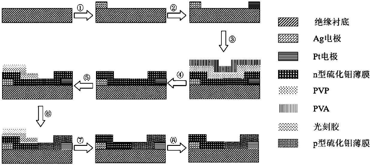
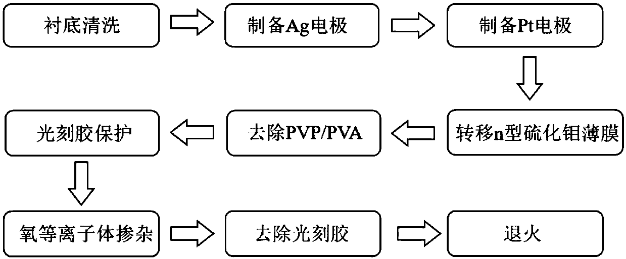
[0033] A method for preparing a transition metal chalcogenide film lateral homojunction of the present invention comprises the following steps:

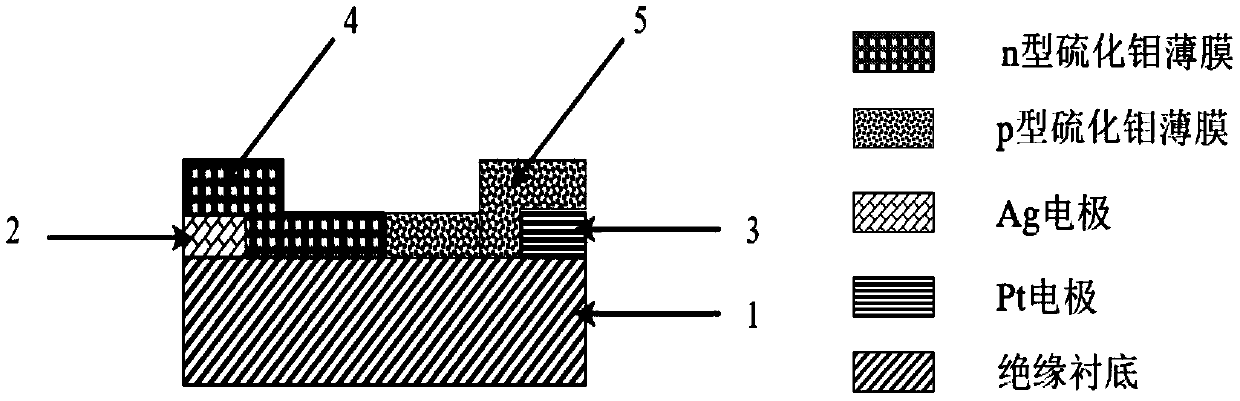
[0034] (1) Electrode A is evaporated on one end of the insulating surface of the insulating substrate A, and electrode B is evaporated on the other end, and the electrode A and the electrode B are not in contact with each other to obtain a sample A;

[0035] (2) Prepare an n-type transition metal chalcogenide film on a silicon substrate B with a silicon dioxide insulating layer, spin-coat the sol on the n-type transition metal chalcogenide film, and then apply the colloid and the lower n-type transition The metal chalcogenide film is torn off, transferred to the sample A described in step (1), and then the sol is removed to obtain a sample B; the two ends of the n-type transition metal chalcogenide film are respectively located on the top of electrode A and electrode B, making part of the electrode A and at least part of the electrod...

Embodiment 1

[0057] The preparation method of the molybdenum sulfide film lateral homojunction solar cell provided by the present invention, the specific steps are as follows:

[0058] (1) Clean two silicon wafers with a silicon dioxide insulating layer on one side, and the thickness of the silicon dioxide insulating layer is 50 nm. Place it in deionized water, ultrasonically clean it for 3 minutes, then place it in acetone solution, ultrasonically clean it for 3 minutes, then place it in absolute ethanol, and ultrasonically clean it for 3 minutes. The two pieces are marked as A and B respectively.

[0059] (2) Place the mask of the corresponding Ag electrode structure on A, and use the electron beam evaporation process to evaporate the Ag electrode with a thickness of 10nm to obtain sample C;

[0060] (3) Place the mask of the corresponding Pt electrode structure on C, and use the electron beam evaporation process to evaporate the Pt electrode with a thickness of 10nm to obtain sample D; ...

Embodiment 2

[0069] The preparation method of the molybdenum sulfide film lateral homojunction solar cell provided by the present invention, the specific steps are as follows:

[0070] (1) Clean two silicon wafers with a silicon dioxide insulating layer on one side, and the thickness of the silicon dioxide insulating layer is 70 nm. Place it in deionized water, ultrasonically clean it for 5 minutes, then place it in acetone solution, ultrasonically clean it for 5 minutes, then place it in absolute ethanol, and ultrasonically clean it for 5 minutes. The two pieces are marked as A and B respectively.

[0071] (2) Place the mask of the corresponding Ag electrode structure on A, and use the electron beam evaporation process to vapor-deposit the Ag electrode with a thickness of 20nm to obtain sample C;

[0072] (3) Place the mask of the corresponding Pt electrode structure on C, and use the electron beam evaporation process to evaporate the Pt electrode with a thickness of 20nm to obtain sample...


PUM


Abstract

The invention discloses a transition metal chalcogenide compound horizontal homogeneous junction solar cell and a preparation method thereof, and belongs to the field of semiconductor materials. The solar cell comprises an insulating substrate, an electrode A, an electrode B, an n-type transition metal chalcogenide compound film and a p-type transition metal chalcogenide compound film; the electrode A and the electrode B are located at the two ends of the insulating substrate respectively; and the n-type transition metal chalcogenide compound film and the p-type transition metal chalcogenide compound film are composed of the same compound, and are transversely connected to form a p-n junction. The method adopts a laser synthesis method to prepare the n-type transition metal chalcogenide compound film, and by virtue of the horizontal homogeneous p-n junction, the lattice mismatch rate of p-n junction is effectively lowered, and the interface defects are reduced; the electrodes are matched with a thin film work function to form high ohmic contact; and the electrodes and the thin films are combined by van der waals force, so that damage of an electrode preparation process to the thinfilms can be effectively avoided, the caused problems of stress, metal diffusion and the like are solved, and the conversion efficiency of the solar cell applying the thin films is improved.

Description

technical field [0001] The invention belongs to the field of semiconductor materials, and more specifically relates to a transition metal chalcogenide lateral homojunction solar cell and a preparation method thereof. Background technique [0002] With the increasing demand for energy and the strengthening of environmental protection around the world, the promotion and application of clean energy has become an inevitable trend. Clean and renewable energy is divided into ocean energy, solar energy, wind energy, hydrogen energy, biomass energy, geothermal energy, etc. Among them, solar energy converts the sun's light energy into other forms of heat energy, electrical energy, and chemical energy. During the energy conversion process, no other harmful gases or solid wastes are produced. It is an environmentally friendly, safe, and pollution-free new energy source. [0003] Vertically stacked van der Waals layered 2D materials have attracted extensive attention due to their excel...

Claims


Application Information

Patent Timeline
Patent Type & Authority Applications(China)
IPC IPC(8): H01L31/068H01L31/032H01L31/0224H01L31/18
CPCH01L31/022425H01L31/032H01L31/068H01L31/18Y02E10/547Y02P70/50
Inventor 曾祥斌靳雯周广通胡一说任婷婷吴少雄王文照郭振宇曾洋肖永红
Owner HUAZHONG UNIV OF SCI & TECH
Why Eureka
Try Eureka