
Integrated circuits and methods for fabricating integrated circuits with improved contact structures

Active Publication Date: 2014-11-06
GLOBALFOUNDRIES US INC
View PDF2 Cites 66 Cited by
  • Summary
  • Abstract
  • Description
  • Claims
  • Application Information

AI Technical Summary

Benefits of technology

The patent provides methods and integrated circuits for making devices with contact structures. The methods involve depositing a hardmask over the contact structure and etching the hardmask to make a via opening that exposes the barrier layer and plug metal. The contact structure is designed to prevent the wet etchant from etching the barrier layer. The via opening is then filled with a conductive material to form an interconnect to the contact structure. The integrated circuits have a contact structure made of fluorine-free tungsten or tungsten carbide and a dielectric material overlaying the semiconductor substrate, with an interconnect formed within the dielectric material and in electrical contact with the contact structure. The methods and circuits improve the reliability and performance of semiconductor devices.

Problems solved by technology

As scaling of semiconductor devices continues, it becomes more difficult to achieve the necessary critical dimensions for vias and trenches.
Therefore, it may be difficult or impossible to use a wet etchant to selectively remove titanium nitride hardmasks after performing a dual damascene process that exposes a metal contact structure including a titanium nitride barrier metal.
Specifically, the etchant will attack and form voids in the metal contact structure during removal of the metal hardmask.
Alternatively, the same metals cannot be used for the metal hardmask and in the metal contact structure.

Method used


Image

  • Integrated circuits and methods for fabricating integrated circuits with improved contact structures
  • Integrated circuits and methods for fabricating integrated circuits with improved contact structures
  • Integrated circuits and methods for fabricating integrated circuits with improved contact structures

Examples


Embodiment Construction

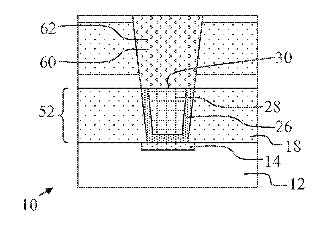
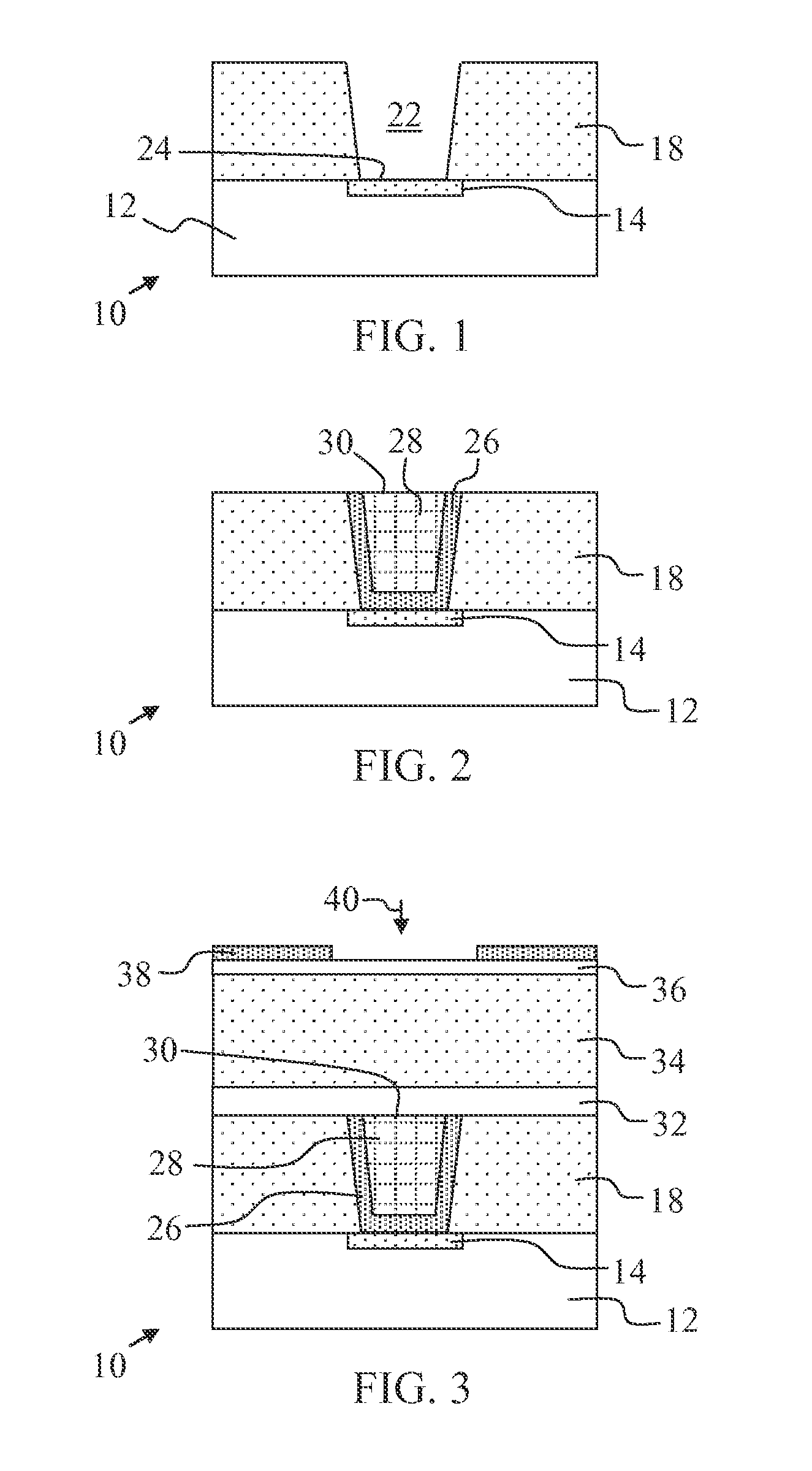
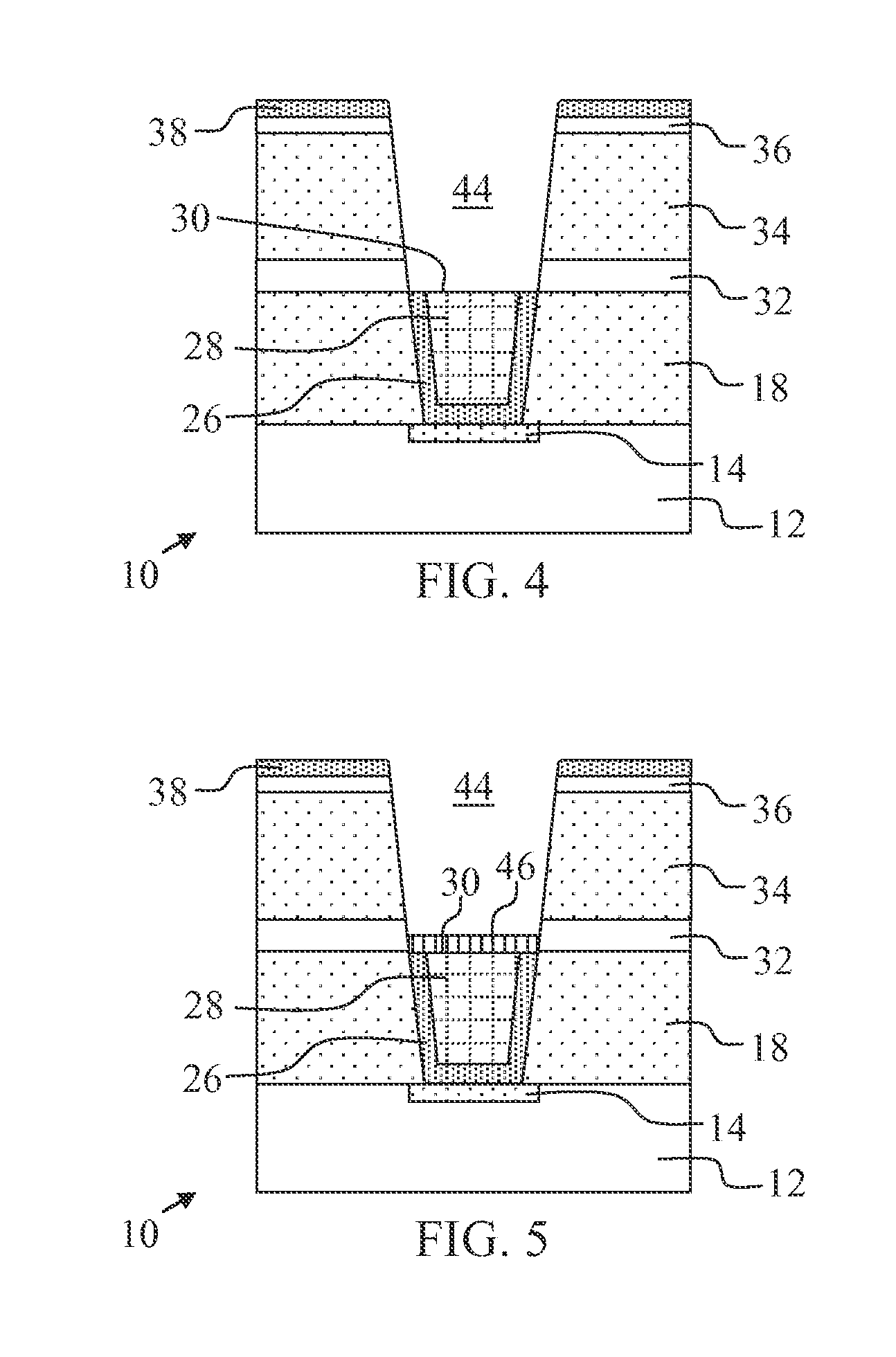
[0013]The following detailed description is merely exemplary in nature and is not intended to limit the integrated circuits or the methods for fabricating integrated circuits claimed herein. Furthermore, there is no intention to be bound by any expressed or implied theory presented in the preceding technical field, background or brief summary, or in the following detailed description.

[0014]Integrated circuits and methods for fabricating integrated circuits with improved contact structures as described herein avoid issues faced by conventional processes for forming interconnects. For example, the methods described herein inhibit etching of contact structure barrier layers during interconnect via formation processes. Specifically, the methods described herein provide for use of a hardmask to etch a via, and for subsequent removal of the hardmask with a wet etchant. The methods described herein further inhibit etching by this wet etchant of the contact structure barrier layer exposed b...


PUM


Abstract

Integrated circuits and methods for fabricating integrated circuits are provided. In an exemplary embodiment, a method for fabricating integrated circuits includes providing a semiconductor substrate disposed with a device therein and / or thereon. A contact structure including a barrier layer and a plug metal overlying the barrier layer is formed in electrical contact with the device. A hardmask is formed overlying the contact structure. The method includes performing an etch to form a via opening through the hardmask and to expose the barrier layer and the plug metal. Further, the method removes a remaining portion of the hardmask with a wet etchant, while the contact structure is configured to inhibit the wet etchant from etching the barrier layer. In the method, the via opening is filled with a conductive material to form an interconnect to the contact structure.

Description

TECHNICAL FIELD[0001]The technical field generally relates to integrated circuits and methods for fabricating integrated circuits, and more particularly relates to integrated circuits and methods for fabricating integrated circuits with contact structures that inhibit etching of contact structure barrier layers.BACKGROUND[0002]Photoresist masks are commonly used in the semiconductor industry to pattern materials such as semiconductors or dielectrics. For example, photoresist masks are used in a dual damascene process to form metal interconnects during the back end of line (BEOL) metallization of a semiconductor device. The dual damascene process involves formation of a photoresist mask on a dielectric layer overlying a metal contact structure or metal conductive layer, such as a tungsten layer. The dielectric layer is then etched according to the photoresist mask to form a via and / or trench that expose the underlying metal contact structure or metal conductor layer. The via and tren...

Claims


Application Information

Patent Timeline
IPC IPC(8): H01L21/768H01L23/48
CPCH01L21/76843H01L23/481H01L21/76802H01L21/28562H01L23/485H01L21/76814H01L21/76849H01L21/31144H01L21/32134H01L2924/0002H01L23/53266H01L2924/00H01L23/528H01L23/53209H01L23/53228H01L23/53295
Inventor ZHANG, XUNYUANLIN, XUANKAMINENI, VIMAL
Owner GLOBALFOUNDRIES US INC
Features
  • Generate Ideas
  • Intellectual Property
  • Life Sciences
  • Materials
  • Tech Scout
  • Unparalleled Data Quality
  • Higher Quality Content
  • 60% Fewer Hallucinations
Learn More