Photodetector circuit
a photodetector and circuit technology, applied in the direction of electrical equipment, semiconductor devices, radio control devices, etc., can solve the problems of deviation and noise, and achieve the effect of reducing deviation
- Summary
- Abstract
- Description
- Claims
- Application Information
AI Technical Summary
Benefits of technology
Problems solved by technology
Method used
Image

Examples
embodiment 1
[0017]In the present specification, the term “a photosensor” refers to a circuit having a semiconductor device converting light energy into electric energy. For example, the semiconductor device includes a device that generates a current according to the quantity of received light and a device, electric resistance of which varies according to an intensity of the received light, etc.
Configuration of Photodetector Circuit 1
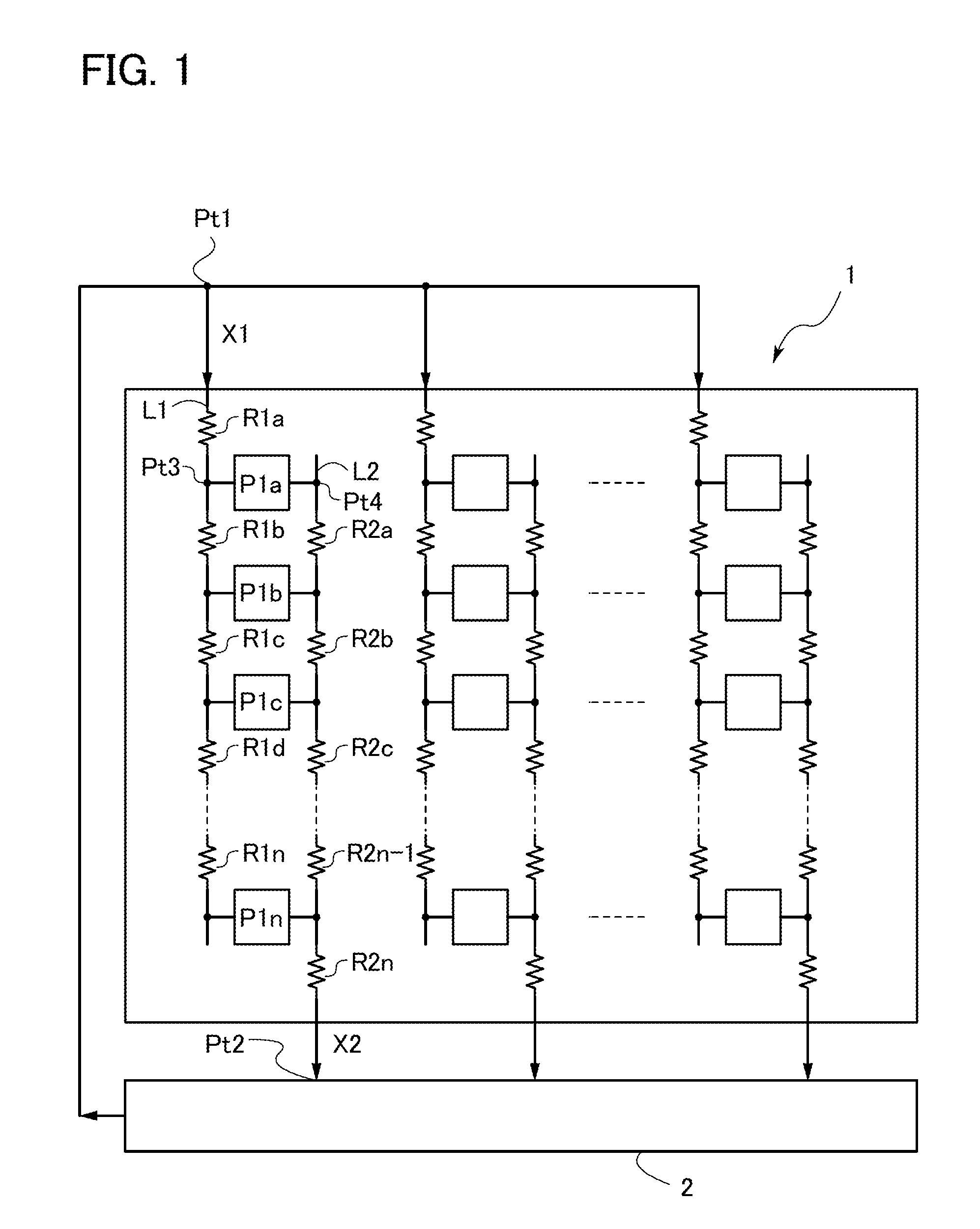
[0018]FIG. 1 shows the constitution of a photodetector circuit 1. In the photodetector circuit 1, a plurality of photosensors are disposed in the shape of a matrix.
[0019]A reference signal line L1 supplies a reference voltage X1 to n photosensors P1a, P1b, . . . P1n disposed in one column. Further, a photosensor output signal line L2 outputs an output signal X2 of the n photosensors P1a, P1b, . . . P1n disposed in a column.
[0020]Here, the reference voltage X1 is supplied to the reference signal line L1 via a wiring disposed from a control circuit 2 located outside o...
embodiment 2
[0045]An example of constructing a circuit of a photosensor will be described with reference to the drawings.
Circuit Configuration of Photosensor P10
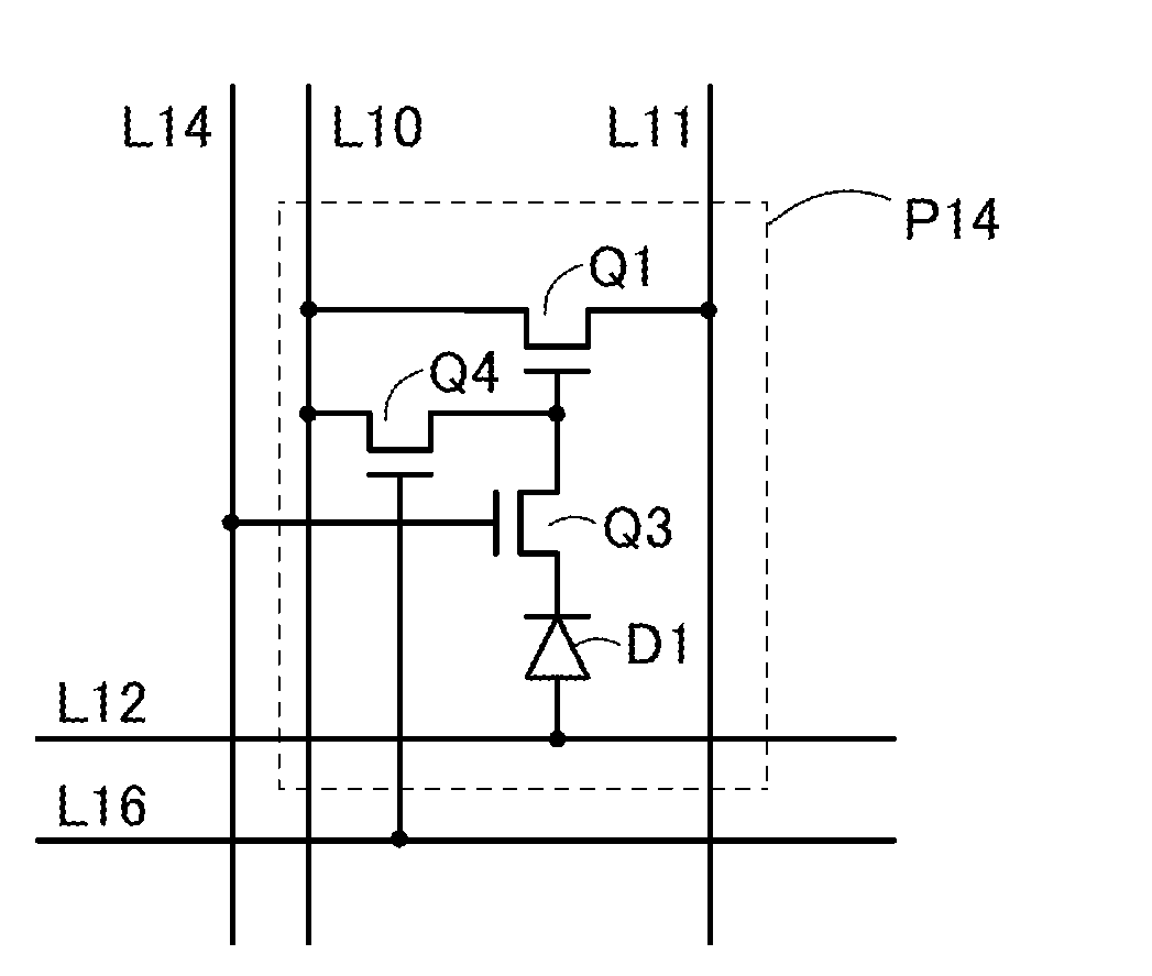
[0046]The constitution of a circuit of a photosensor P10 will be described with reference to FIG. 3A. This photosensor P10 includes a photodiode D1 and transistors Q1 and Q2.
[0047]In the photodiode D1, an anode is connected to a wiring L12, and a cathode is connected to a gate of the transistor Q1.
[0048]In the transistor Q1, one of a source and a drain is connected to the reference signal line L10 and the other of the source and the drain is connected to one of a source and a drain of the transistor Q2.
[0049]In the transistor Q2, a gate is connected to a wiring L13 and the other of the source and the drain of the transistor Q2 is connected to a photosensor output signal line L11.
[0050]The transistor Q1 generates an output signal of the photosensor P10 according to the amount of electrical charge supplied from the photodiode D1. Further,...
embodiment 3
[0077]One example of a manufacturing method of a transistor using a highly purified and electrically i-typed (intrinsic-typed) oxide semiconductor will be explained with reference to FIGS. 6A to 6E.
[0078]First, an insulating layer 101 is formed as a base layer over a substrate 100. The insulating layer 101 is formed by removing residual moisture from a treatment chamber. This is to prevent hydrogen, water, hydroxyl, or hydroxide, etc. from being be included in the insulating layer 101.
[0079]Next, an oxide semiconductor layer is formed over the insulating layer 101 by sputtering. Before forming the oxide semiconductor layer, the substrate 100 with the insulating layer 101 thereover is pre-heated. This is to prevent hydrogen, moisture, and hydroxyl from being included in the oxide semiconductor layer as much as possible. Impurities such as hydrogen, moisture, etc. absorbed in the substrate 100 are removed and exhausted.
[0080]A metal oxide sputtering target comprising zinc oxide as a m...
PUM
 Abstract
Description
Claims
Application Information
 - R&D
- Intellectual Property
- Life Sciences
- Materials
- Tech Scout
- Unparalleled Data Quality
- Higher Quality Content
- 60% Fewer Hallucinations
Browse by: Latest US Patents, China's latest patents, Technical Efficacy Thesaurus, Application Domain, Technology Topic, Popular Technical Reports.
© 2025 PatSnap. All rights reserved.Legal|Privacy policy|Modern Slavery Act Transparency Statement|Sitemap|About US| Contact US: help@patsnap.com