

Semiconductor device
- Summary
- Abstract
- Description
- Claims
- Application Information
AI Technical Summary
Benefits of technology
Problems solved by technology
Method used
Image

Examples
Embodiment Construction
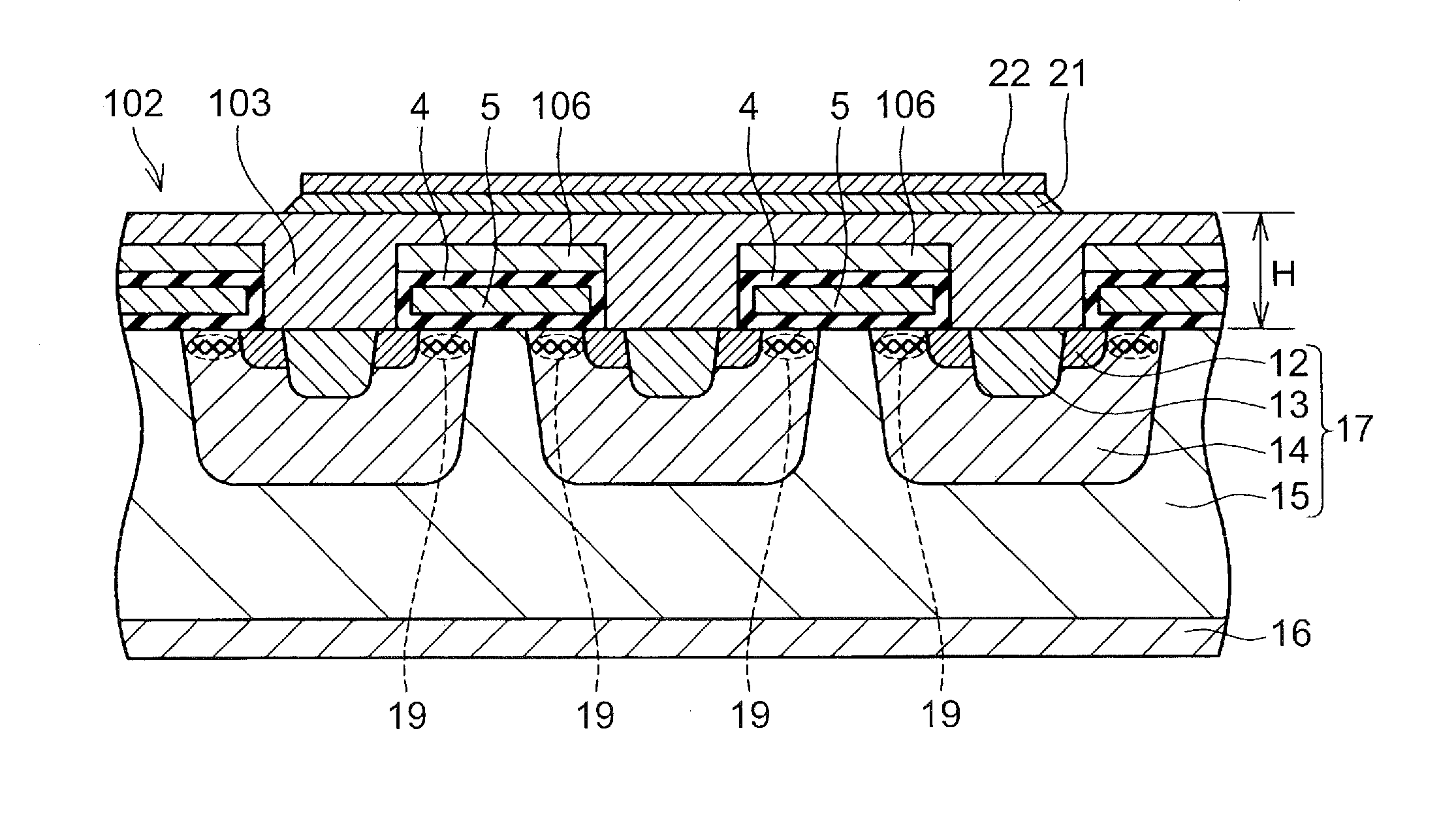
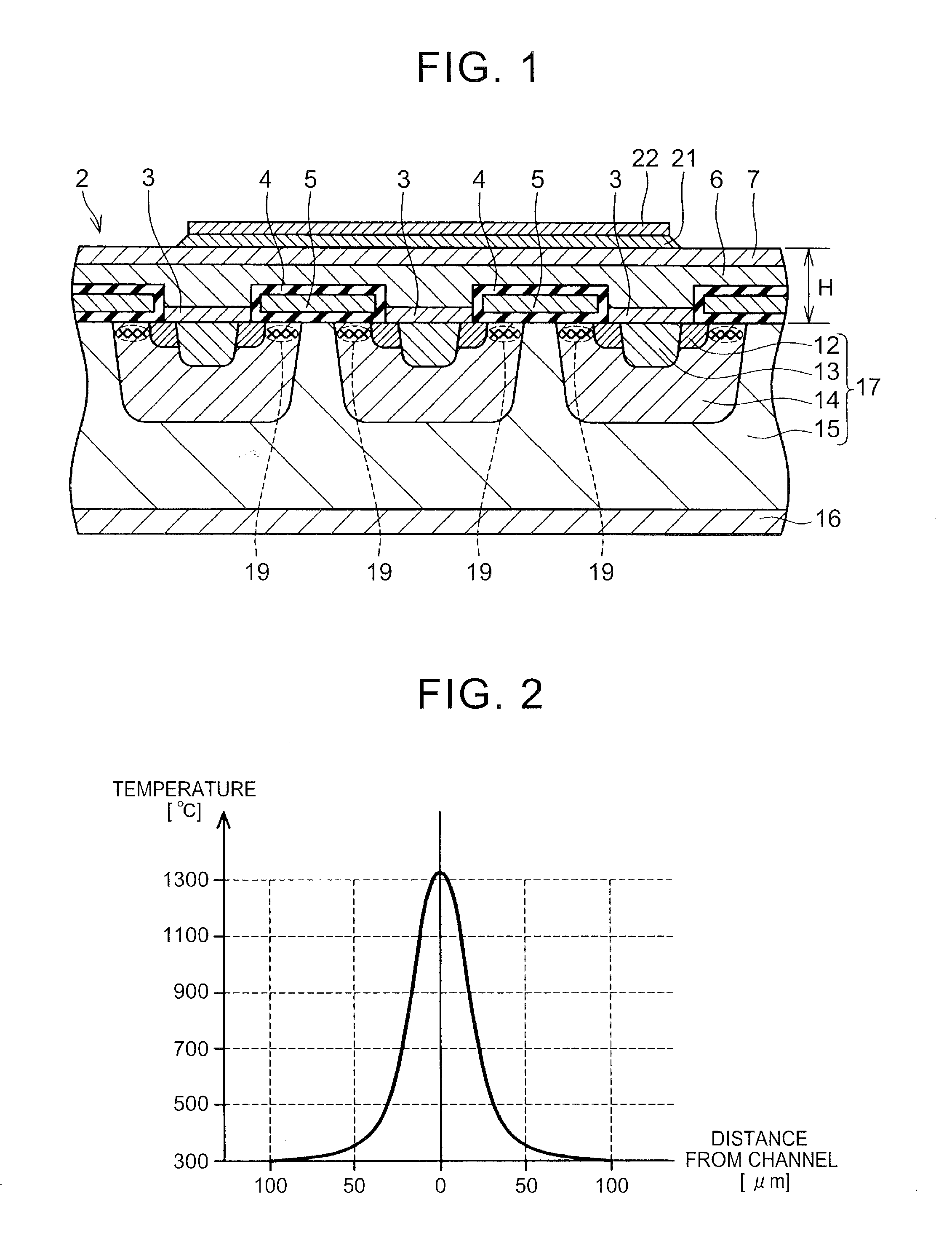
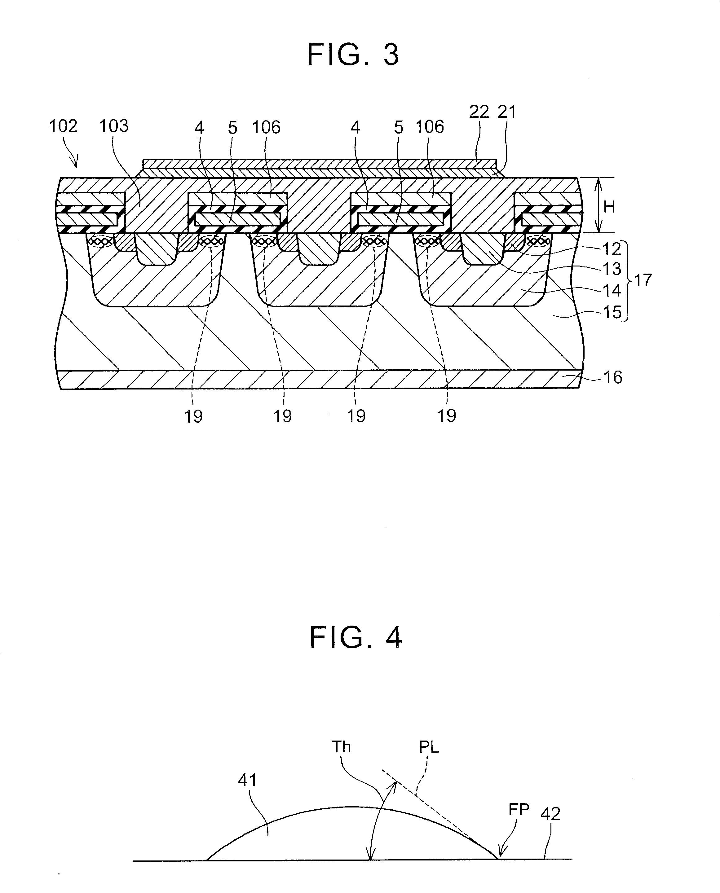
[0017]At first, an outline of an embodiment of the present invention will be described. A semiconductor device that is an embodiment of the present invention includes a first electrode, a second electrode, and an endothermic layer. The first electrode, the second electrode and the endothermic layer are formed on a semiconductor substrate. The first electrode is directly connected and electrically conductive with an element formed inside of the semiconductor substrate. More specifically, the first electrode is electrically conductive with the element on a surface of the semiconductor substrate. The endothermic layer is in contact with the first electrode. The second electrode is in contact with at least one of the first electrode and the endothermic layer, and is soldered to a metal electric conductor. Herein, the metal electric conductor may be a joining member for electrically joining other device electrically connected to the semiconductor device and the semiconductor device, and ...
PUM
 Abstract
Description
Claims
Application Information