Method of forming strained source and drain regions in a p-type finfet structure

Active Publication Date: 2014-12-04
SHANGHAI HUALI MICROELECTRONICS CORP
View PDF10 Cites 3 Cited by
  • Summary
  • Abstract
  • Description
  • Claims
  • Application Information

AI Technical Summary

Benefits of technology

The present invention provides a method for forming strained source and drain regions in a P-type FinFET structure with uniform stressors and well-controlled scope. This method improves carrier mobility and reduces current leakage without affecting the structure of the FinFET. In addition, the embedded stressors become more uniform and the range of the stressors becomes more controllable.

Problems solved by technology

However, compared to the embedded silicon germanium (e-SiGe) PMOS process for increasing the carrier mobility of the PMOS device, it is much more difficult to form stressors in source / drain region of a p-type FinFET since the conventional method may cause the deformation of the FinFET structure and the nonuniformity of the stressors in source / drain region.
Although simple, such method may lead to the structural deformation of the FinFET.
Morever, in the known method, the SiGe does not grow uniformly by epitaxial growth and the scope of the embedded SiGe is difficult to control.

Method used


Image

  • Method of forming strained source and drain regions in a p-type finfet structure
  • Method of forming strained source and drain regions in a p-type finfet structure
  • Method of forming strained source and drain regions in a p-type finfet structure

Examples


Embodiment Construction

[0026]The method of forming strained source and drain regions in a P-type FinFET of the present invention will be described in further details hereinafter with respect to the embodiments and the accompanying drawings.

[0027]The present invention is described with reference to the attached figures, wherein like reference numerals are used throughout the figures to designate similar or equivalent elements. The figures are not drawn to scale and they are provided merely to illustrate the invention.

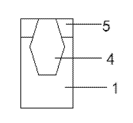
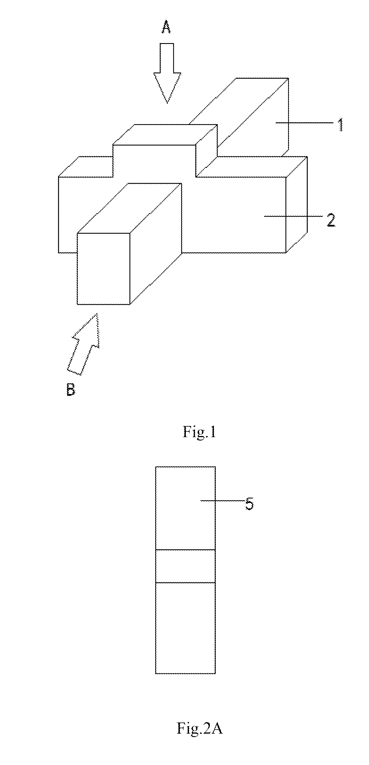
[0028]Referring to FIG. 1, the P-type FinFET structure comprises a gate 2 and a fin 1 having a channel region and source and drain regions extending from the channel region. The fin comprises a first semiconductive material. In the embodiment, the first semiconductive material is single crystalline silicon, and thus the source and drain regions are both filled with the single crystalline silicon material. The gate comprises mono-crystalline silicon.

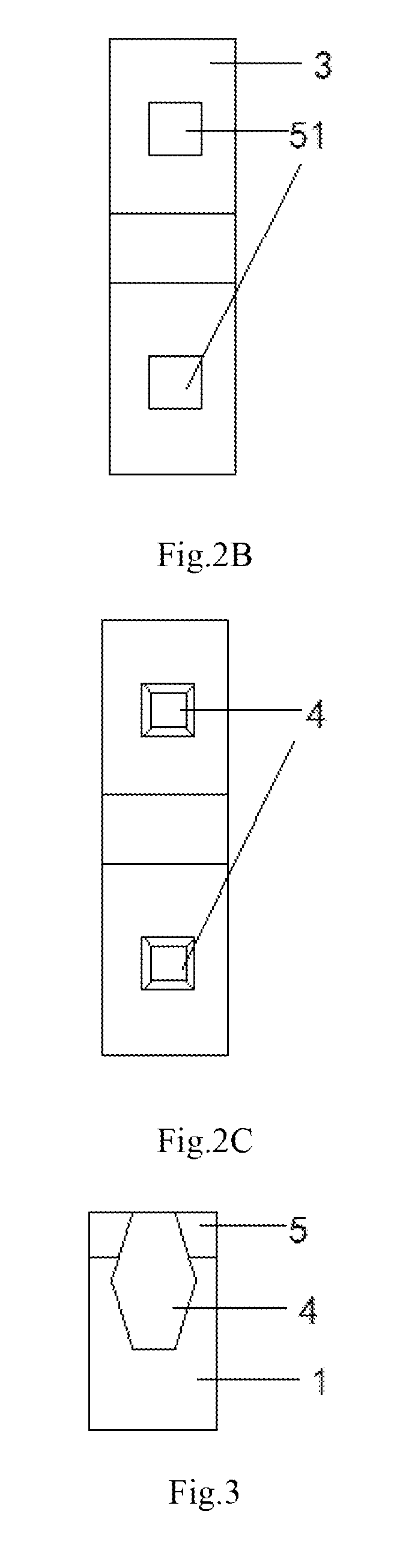
[0029]Referring to FIG. 2a to FIG. 2c, which ...


PUM


Abstract

A method of forming strained source and drain regions in a P-type FinFET structure is disclose. The method comprises depositing an isolation layer on the FinFET structure; applying a lithography and etching process to expose the isolation layer in two areas on opposite sides of the gate over the source / drain region of the FinFET, and etching through the exposed isolation layer to expose the semiconductive material of the source / drain region in the two areas; forming a recess in each of the source / drain region from the exposed semiconductive material; selectively epitaxially growing another semiconductive material in the recesses to increase the source / drain strain; and removing the rest of the isolation layer.

Description

CROSS-REFERENCE TO RELATED APPLICATION[0001]This application claims the priority benefit of China application serial no. 201310213628.5, filed May 31, 2013. All disclosure of the China application is incorporated herein by reference.FIELD OF THE INVENTION[0002]The present invention relates to the field of semiconductor fabrication technology and particularly to a method of forming strained source and drain regions in a P-type finFET structure.BACKGROUND OF THE INVENTION[0003]With the development of the semiconductor technology, fin field effect transistors (FETs) represent new CMOS devices for improving FET performance. The gate of a conventional planar transistor is located over the channel on one side, while the gate of a FinFET surrounds the channel from two sides, thus electrostatic control may be implemented for the channel from two sides. By such design, the FinFET can improve the control over the channel, reduce short-channel effect, and reduce the gate length effectively. Ho...

Claims


Application Information

Patent Timeline
IPC IPC(8): H01L29/66H01L21/02
CPCH01L29/66795H01L21/02428H01L21/02658H01L21/02587H01L21/02532H01L29/7848H01L29/785
Inventor DING, YIZHANG, MINGHUAFANG, JINGXUNYAN, JUNHUA
Owner SHANGHAI HUALI MICROELECTRONICS CORP
Why Eureka
Try Eureka