Latch-up free vertical tvs diode array structure using trench isolation

a diode array and trench isolation technology, applied in the direction of diodes, semiconductor devices, electrical equipment, etc., can solve the problems of sudden and strong voltage snapback, parasitic pnp and npn transistors, undesirable effects of system instability or even damage, etc., to prevent the latch-up of parasitic pnp

Active Publication Date: 2014-12-11
ALPHA & OMEGA SEMICON INC
View PDF3 Cites 22 Cited by
  • Summary
  • Abstract
  • Description
  • Claims
  • Application Information

AI Technical Summary

Benefits of technology

[0014]The present invention further discloses a method for manufacturing an electronic device with an integrated transient voltage-suppressing (TVS) array. The method includes a step of manufacturing the TVS array in a semiconductor substrate by doping a plurality of dopant regions of different conductiv

Problems solved by technology

The conventional technologies for designing and manufacturing a transient voltage suppressor (TVS) array is still confronted with a technical difficulty that the in a TVS array wherein multiple PN junctions diodes are manufactured in a semiconductor substrate by applying a standard COMS processing steps, there are inherent PNP and NPN parasitic transistors.
In an ESD event or the occurrence of a transient voltage, with a larger voltage applied to this TVS array, the parasitic NPN or PNP transistors are turned on and latched up, thus causing a sudden and strong voltage snap back.
The sudden and large snapback may cause the undesirable effects of system instability or even damages.
Additionally, the latch-up of the parasitic NPN or PNP transistors in the TVS array may further lead to other unexpected or undesirable voltage-current transient conditions.
The technical difficulties caused by the parasitic PNP or NPN latch-up in the TVS array cannot be easily resolved.
However, in situations such as electrostatic discharge (ESD), electrical fast transients and lightning, an unexpected and an uncontrollable high voltage may accidentally strike onto the circuit.
However, the PN junction type of TVS has no

Method used


Image

  • Latch-up free vertical tvs diode array structure using trench isolation
  • Latch-up free vertical tvs diode array structure using trench isolation
  • Latch-up free vertical tvs diode array structure using trench isolation

Examples


Embodiment Construction

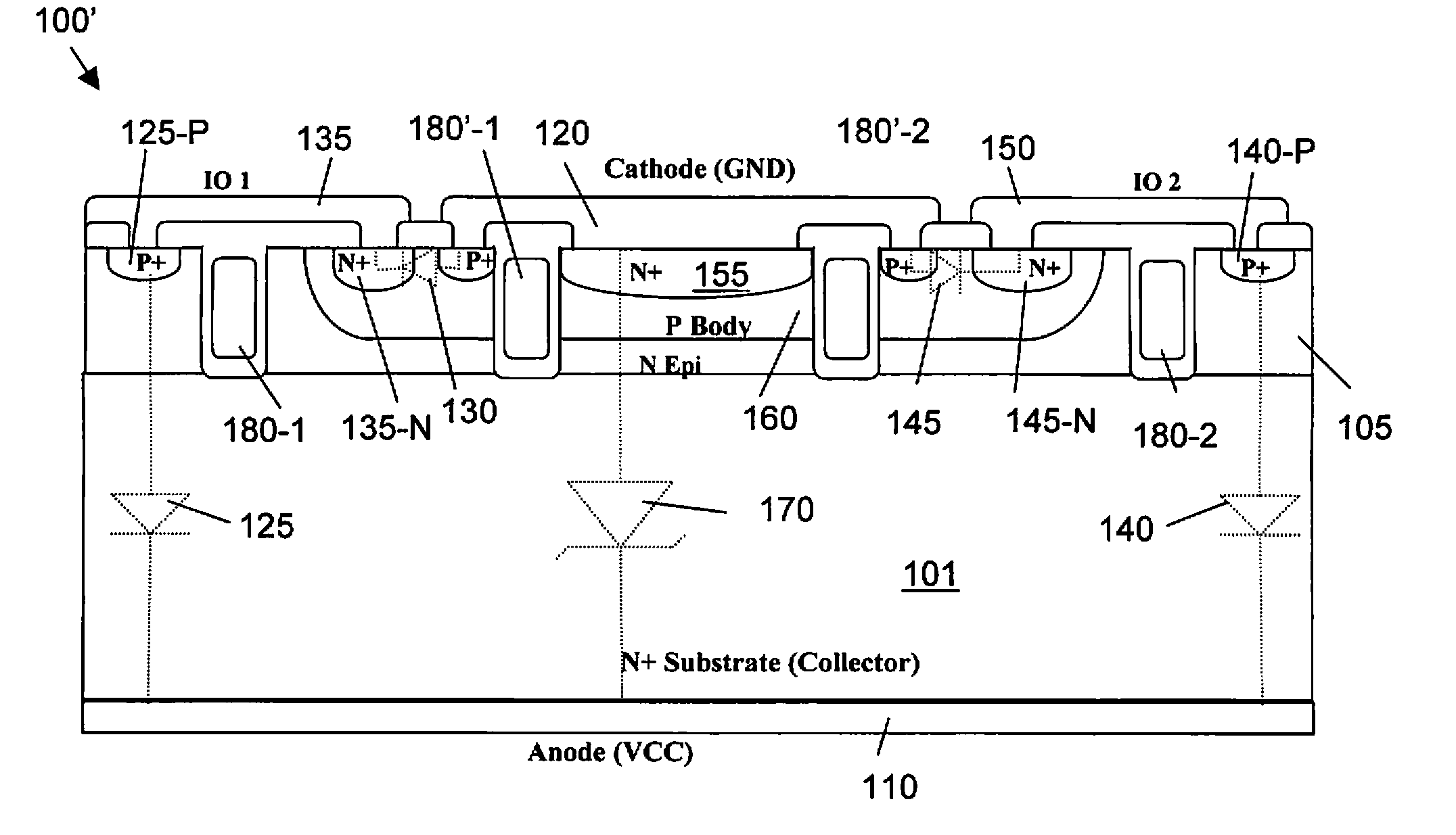
[0025]Referring to FIG. 4 for a side cross sectional view of a new and improved implementation a part of TVS array of this invention. The partial TVS array 100 as shown with two channels is supported on a N-epi layer 105 on top of a N+ substrate 101 with the bottom surface connected to an anode terminal 110 at a Vcc voltage. The TVS array is connected between the anode 110 disposed at the bottom surface and a cathode terminal 120 disposed at a top surface connected to a ground voltage. The TVS array 100 further includes a first high side diode 125 and a first low side diode 130 connected to a first IO terminal 135. The TVS array 100 further includes a second low side diode 140 and a second low side diode 145 connected to a second IO terminal 150. The first high side diode 125 is formed as a PN junction between the P+ doped region 125-P and the N-epi 105. The first low side diode 130 is formed as a PN junction between an N+ region 135-N and a P-body region 160 disposed below the cath...


PUM


Abstract

A method for manufacturing a transient voltage suppressing (TVS) array substantially following a manufacturing process for manufacturing a vertical semiconductor power device. The method includes a step of opening a plurality of isolation trenches in an epitaxial layer of a first conductivity type in a semiconductor substrate followed by applying a body mask for doping a body region having a second conductivity type between two of the isolation trenches. The method further includes a step of applying an source mask for implanting a plurality of doped regions of the first conductivity type constituting a plurality of diodes wherein the isolation trenches isolating and preventing parasitic PNP or NPN transistor due to a latch-up between the doped regions of different conductivity types.

Description

[0001]This Patent Application is a Continuous Application and claims the Priority Date of a co-pending application Ser. No. 13 / 421,608 filed by common Inventors of this Application on Mar. 15, 2012. Application Ser. No. 13 / 421,608 is a Divisional Application and claims the Priority Date of another Application Ser. No. 12 / 931,434 filed on Feb. 1, 2011 and another application Ser. No. 11 / 606,602, now issued as U.S. Pat. No. 7,880,223, filed on Nov. 30, 2006 by common Inventors of this Application. The Disclosures made in the patent application Ser. Nos. 13 / 421,608, 11 / 606,602 and 12 / 931,434 are hereby incorporated by reference.BACKGROUND OF THE INVENTION[0002]1. Field of the Invention[0003]The invention relates generally to a circuit configuration and method of manufacturing a transient voltage suppressor (TVS). More particularly, this invention relates to an improved circuit configuration and method of manufacturing vertical TVS array implemented with trench isolation for resolving a...

Claims


Application Information

Patent Timeline
IPC IPC(8): H01L29/866
CPCH01L29/866H01L27/0255H01L27/0744H01L27/075H01L27/0761H01L29/0649H01L29/861H01L27/0755H01L29/7416
Inventor BOBDE, MADHUR
Owner ALPHA & OMEGA SEMICON INC
Why Eureka
Try Eureka