Wiring film and active matrix substrate using the same, and method for manufacturing wiring film

a technology of active matrix substrate and wiring film, which is applied in the direction of basic electric elements, electrical equipment, semiconductor devices, etc., can solve the problems of reducing the breakdown voltage of the insulating film, the inclination of the sidewall of the tapered al wiring film acutely changes accordingly, and the film has poor step coverage characteristics

Inactive Publication Date: 2014-12-25
MITSUBISHI ELECTRIC CORP
View PDF11 Cites 0 Cited by
  • Summary
  • Abstract
  • Description
  • Claims
  • Application Information

AI Technical Summary

Benefits of technology

[0008]It is an object of the present invention to provide a structure of an Al wiring film and a method for manufacturing the same, from which a tapered Al wiring film can be obtained easily and in a stable manner, and which can be applied to an active matrix substrate of a display apparatus.
[0013]According to the present invention, the tapered shape of the Al wiring film can be stabilized without a need to manage the etchant stricter than in the conventional case. Accordingly, the step coverage characteristic of the gate insulating film formed on the Al wiring film is improved, it is possible to prevent the breakdown voltage from reducing and the wiring film in the upper layer from breaking, and the yield of the product is improved. In addition, since the second layer made of an Al alloy containing at least one element of Ni, Pd, and Pt can obtain an excellent contact characteristic with an oxide material used as a transparent pixel electrode, it is easy to apply the wiring film to an electrode of a thin-film transistor provided in an active matrix substrate of a display apparatus.
[0014]According to the present invention, the tapered shape of the Al wiring film can be stabilized without a need to manage the etchant stricter than in the conventional case. Accordingly, the step coverage characteristic of the insulating film formed on the Al wiring film is improved, it is possible to prevent the breakdown voltage from reducing and the wiring film in the upper layer from breaking, and the yield of the product is improved. In addition, since the layer made of an Al alloy containing at least one element of Ni, Pd, and Pt can obtain an excellent contact characteristic with an oxide material used as a transparent pixel electrode, it is easy to apply the wiring film to an electrode of a thin-film transistor provided in an active matrix substrate of a display apparatus.

Problems solved by technology

However, since the method is isotropic etching, a sidewall of an Al wiring film resulted from patterning becomes substantially vertical.
This causes an insulating film formed on the Al wiring film to have a poor step coverage characteristic, and, as a result, causes broken wiring of a wiring film formed on the insulating film, a reduction of a breakdown voltage of the insulating film, or the like.
However, when a composition of a chemical solution (etchant) changes as an etching process progresses or degrades by time in such a technique, an inclination of the sidewall of the tapered Al wiring film acutely changes accordingly.
This poses a problem of a difficulty in managing the composition of the etchant.
This causes the insulating film formed on the Al wiring film to have a poor step coverage characteristic, and, as a result, causes a reduction of a breakdown voltage of the insulating film, broken wiring of the wiring film of an upper layer, or the like, which eventually causes a drop in the yield of the product.
However, it is necessary to severely manage the composition of the etchant to obtain a predetermined tapered shape in a stable manner.
To do so, it is necessary, for example, to introduce a facility to constantly monitor the concentration of the etchant, or replace the etchant more frequently, which eventually increases the cost.
Further, when an ordinary Al film is used as an electrode of a thin-film transistor (TFT) of an active matrix substrate for a liquid crystal display apparatus, contact characteristics between the TFT and a pixel electrode are drastically degraded due to an interface reaction with an ITO film which is a transparent pixel electrode.
For this reason, it is difficult to apply the Al wiring film as a wiring film on the active matrix substrate.

Method used


Image

  • Wiring film and active matrix substrate using the same, and method for manufacturing wiring film
  • Wiring film and active matrix substrate using the same, and method for manufacturing wiring film
  • Wiring film and active matrix substrate using the same, and method for manufacturing wiring film

Examples


first preferred embodiment

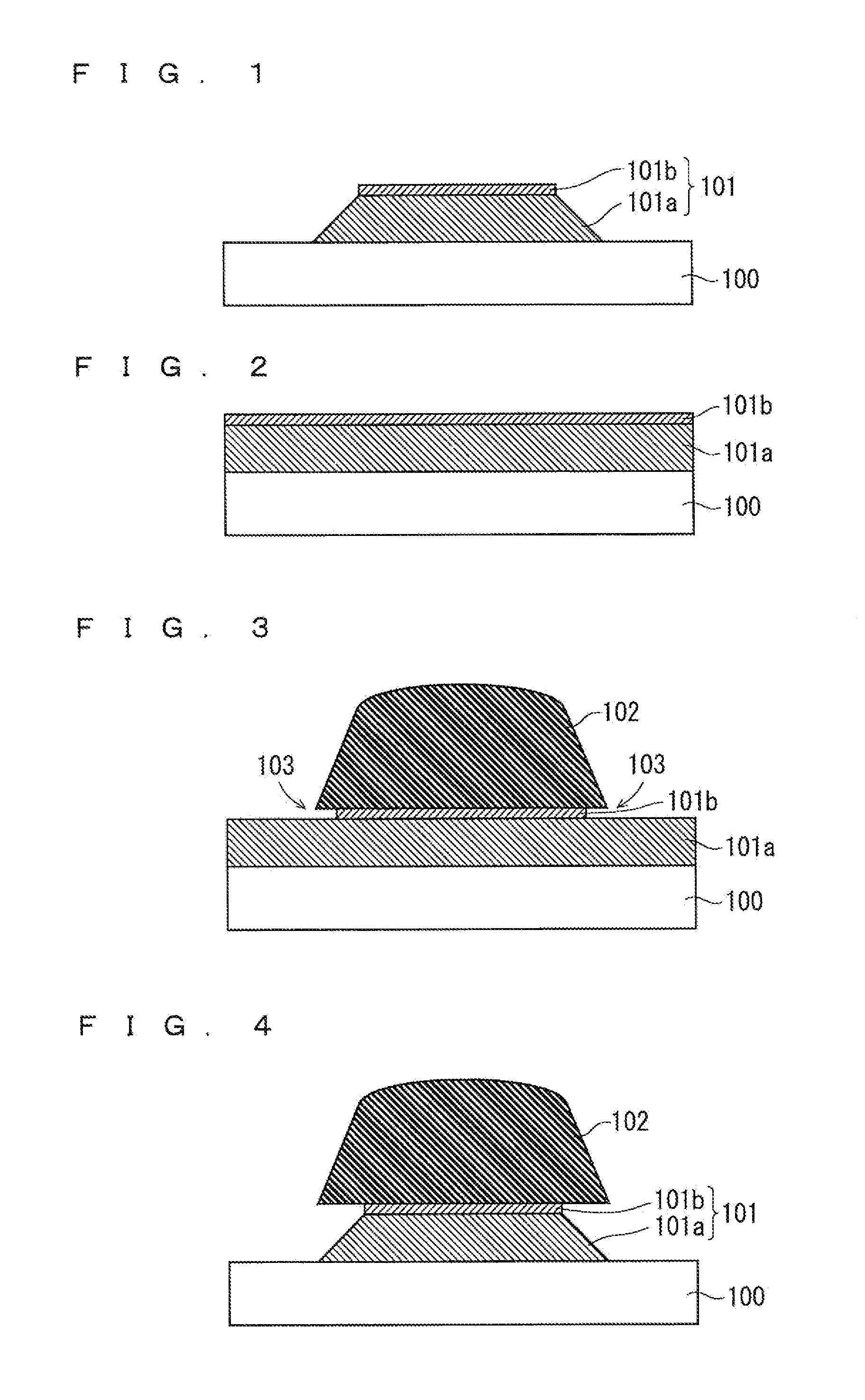
[0025]FIG. 1 is a cross sectional view of a structure of an Al wiring film according to a first preferred embodiment. As illustrated in FIG. 1, an Al wiring film 101 formed on a substrate 100 according to this preferred embodiment has a double-layer structure including a first Al alloy layer 101a and a second Al alloy layer 101b formed thereon, and has a tapered shape in cross section with a width smaller in an upper portion thereof than a width in a bottom portion thereof.

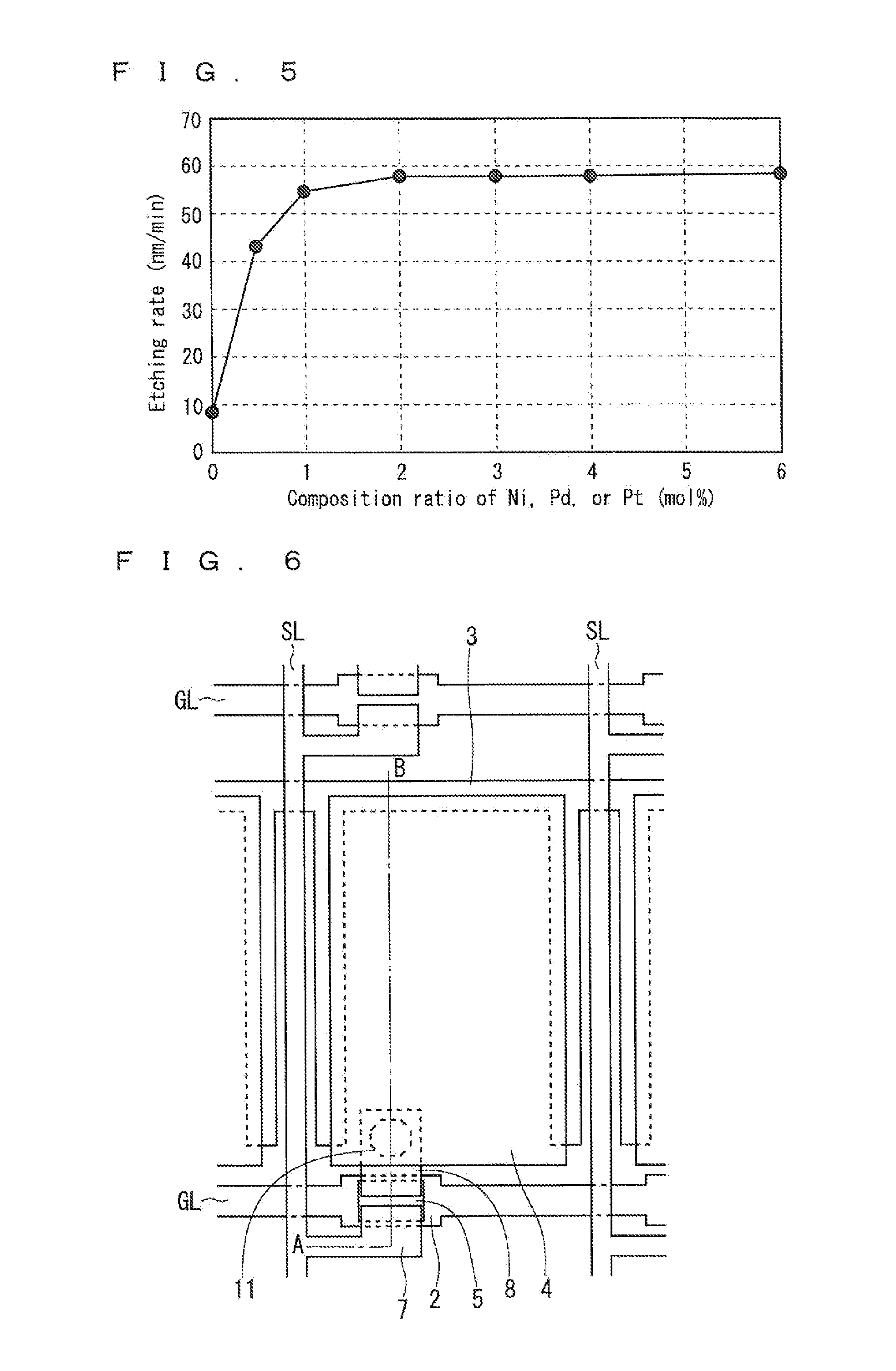
[0026]The first Al alloy layer 101a is a layer including Al as a main component. This is not restricted to the Al alloy, but pure Al may also be used. The second Al alloy layer 101b is made of an Al alloy containing at least one element of nickel (Ni), palladium (Pd), and platinum (Pt). The composition of the Al alloy of the first Al alloy layer 101a is different from the composition of the Al alloy of the second Al alloy layer 101b.

[0027]In addition, the substrate 100 serving as a base for the Al wiring film 101...

second preferred embodiment

[0066]FIG. 12 is a cross sectional view of a structure of an Al wiring film according to a second preferred embodiment. As illustrated in FIG. 12, an Al wiring film 201 formed on a substrate 100 according to this preferred embodiment has a triple-layer structure including a first Al alloy layer 201a, a second Al alloy layer 201b, and a third Al alloy layer 201c which are laminated in this order, and has a tapered shape in cross section with a width smaller in an upper portion thereof than a width in a bottom portion thereof.

[0067]The first Al alloy layer 201a is made of an Al alloy containing at least one element of Ni, Pd, and Pt. The second Al alloy layer 201b is made of an Al alloy containing nitrogen (N). The third Al alloy layer 201c is made of an Al alloy containing at least one element of Ni, Pd, and Pt. The first Al alloy layer 201a and the third Al alloy layer 201c may have an identical composition. Also, the second Al alloy layer 201b may be formed by adding nitrogen to an...


PUM

PropertyMeasurementUnit
thicknessaaaaaaaaaa
thicknessaaaaaaaaaa
thicknessaaaaaaaaaa

Abstract

An Al wiring film having a tapered shape is obtained easily and in a stable manner. An Al wiring film has a double-layer structure including a first Al alloy layer made of Al or an Al alloy, and a second Al alloy layer laid on the first Al alloy layer and having a composition different from a composition of the first Al alloy layer by containing at least one element of Ni, Pd, and Pt. The second Al alloy layer is etched by an alkaline chemical solution used in a developing process of a photoresist, and an end portion of the second Al alloy layer recedes from an end portion of the photoresist. Thereafter, by performing wet etching using the photoresist as a mask, a cross section of the Al wiring film becomes a tapered shape.

Description

FIELD OF THE INVENTION[0001]The present invention relates to a structure of a wiring film containing aluminum and a method for manufacturing the same, and more particularly to a wiring film applicable to an electrode of a thin-film transistor provided on an array substrate or the like of a liquid crystal display apparatus.DESCRIPTION OF THE BACKGROUND ART[0002]For example, aluminum (Al) is known as a material of a wiring film used as an electrode of a thin-film transistor that is formed on an array substrate (active matrix substrate) of a liquid crystal display apparatus. Since an electric resistance of Al is very low, it has been generally used as a wiring material conventionally. In this specification, a film obtained not only from pure Al but also a material containing Al as a main components such as an Al alloy, and a wiring film resulted from patterning such a film are broadly referred to as an “Al film” and an “Al wiring film”, respectively.[0003]A wet etching method using a c...

Claims


Application Information

Patent Timeline
Patent Type & Authority Applications(United States)
IPC IPC(8): H01L21/768H01L21/283
CPCH01L21/283H01L21/76838H01L29/458H01L29/4908H01L27/1244
Inventor FUJIWARA, KAZUYUKIINOUE, KAZUNORIYAMABE, TAKAHITO
Owner MITSUBISHI ELECTRIC CORP
Why Eureka
Try Eureka