
Power Semiconductor Module and Power Module

a technology of power semiconductor modules and power semiconductors, applied in the direction of printed circuit stress/warp reduction, basic electric elements, electrical apparatus construction details, etc., can solve the problems of high capacity, difficult control of on-vehicle motors used in automobiles, etc., and achieve the effect of improving reliability and increasing intimate adhesion strength

Active Publication Date: 2015-01-01
HITACHI ASTEMO LTD
View PDF2 Cites 39 Cited by
  • Summary
  • Abstract
  • Description
  • Claims
  • Application Information

AI Technical Summary

Benefits of technology

The power semiconductor module described in this patent has several advantages. First, the resin sealer that surrounds the conductor plates and semiconductor devices has recesses that improve adhesion between the sealer and a spray coated film. Second, the size of the recesses is chosen to prevent large gaps between the flat portions of the spray coated film, further improving bonding strength. Third, the recesses are shaped so that voids can be reduced, and the insulation film formed on the spray coated film has increased thermal conductivity and adhesion strength with the heat dissipation portions of the module case. Fourth, the insulation sheet is attached under pressure to form the insulation film, improving its insulation and thermal conductivity, and also increasing efficiency in the process. Fifth, the resin layer formed on the insulation film and the conductor plate has reduced stress by including recesses that reflect the shape of the recesses in the resin sealer. These recesses also enhance the stress relaxation effect.

Problems solved by technology

A high-capacity, on-vehicle motor used in an automobile is difficult to drive and control by using a DC voltage from a battery, and an electric power converter that uses switching operation of a power semiconductor device is essentially required for voltage step up and AC control.

Method used


Image

  • Power Semiconductor Module and Power Module
  • Power Semiconductor Module and Power Module
  • Power Semiconductor Module and Power Module

Examples


first embodiment

Overall Structure of Power Module

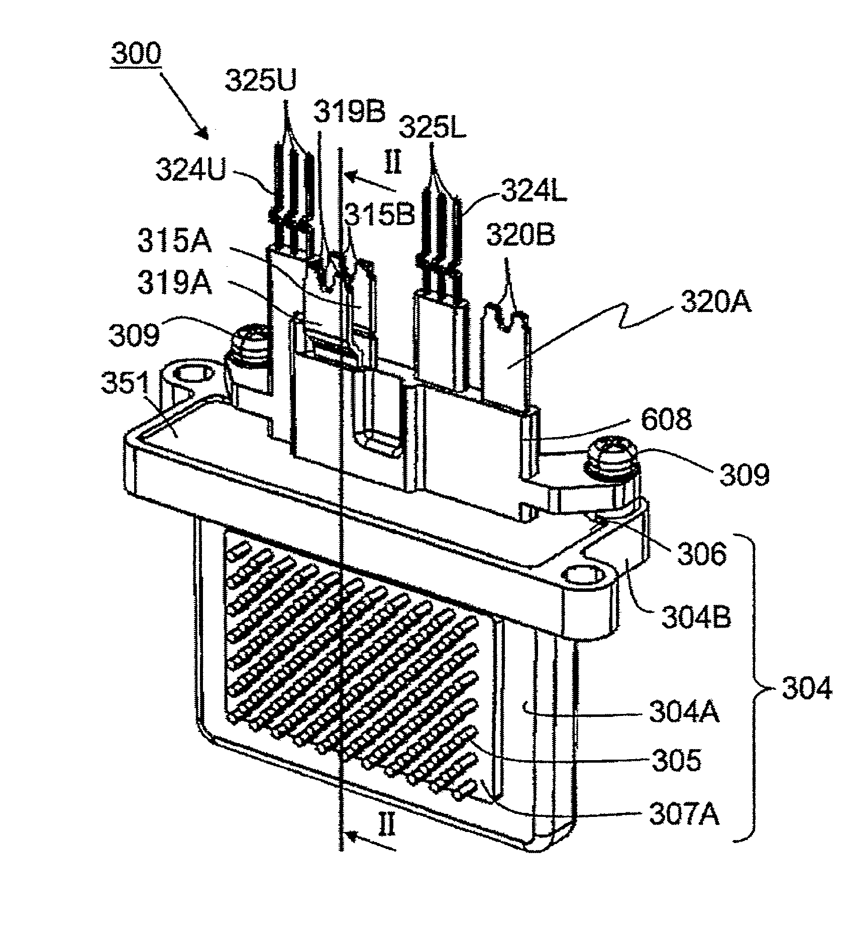
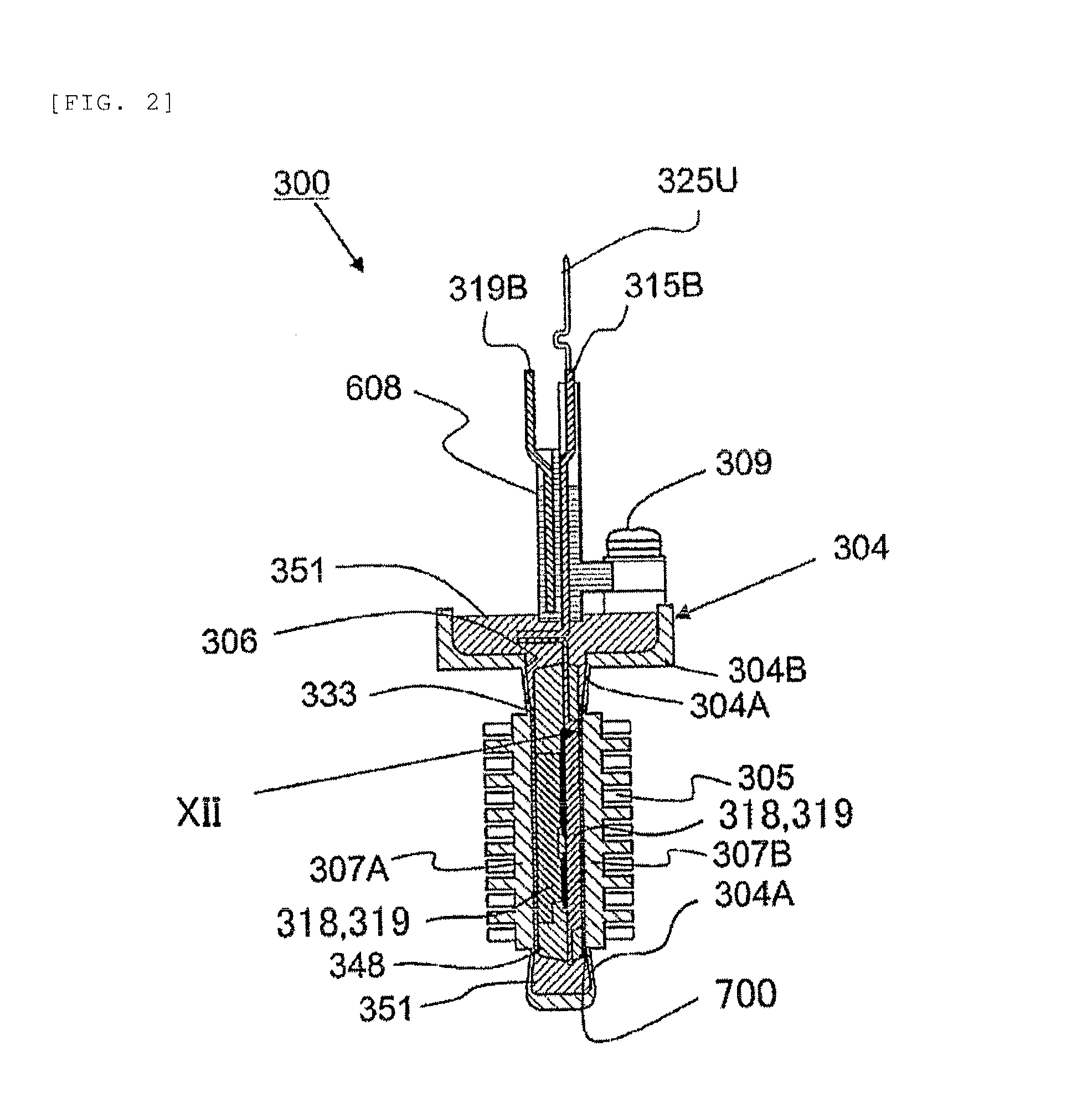
[0051]FIGS. 1 to 15 show a first embodiment of a power semiconductor module according to the invention. FIG. 1 is a perspective view of the external appearance of a power module having the power semiconductor module. FIG. 2 is a cross-sectional view of the power module taken along the line II-II in FIG. 1.

[0052]A power module 300 has a module case 304, which accommodates a power semiconductor module including a switching device and formed in a transfer mold process. The power module 300 is used, for example, in an electric power converter incorporated in an electric automobile, a hybrid automobile, or any other electric vehicle.

[0053]As shown in FIG. 2, the power module 300 has a power semiconductor module 302 shown in FIG. 3 accommodated in the module case (heat dissipation member) 304, which is a CAN-type cooler. The CAN-type cooler is a tubular cooler having an insertion opening 306 (see FIG. 2) on one side and a bottom on the other side. The modu...

second embodiment

[0121]FIG. 21(a) is a cross-sectional view of a structure in which the fillers contained in the resin sealer are not exposed through the surface of each of the recesses, and FIG. 21(b) is a cross-sectional view of a structure according a second embodiment of the invention in which the fillers contained in the resin sealer are exposed through the surface of each of the recesses. As shown in FIG. 21(a), the resin sealer 348 is made of a resin 348G based on a novolac-based, multifunctional-based, biphenyl-based epoxy resin containing ceramic fillers 348F made, for example, of SiO2, Al2O3, AlN, and BN in order to lower the magnitude of thermal stress produced when the semiconductor devices (IGBTs 328, 330 and diodes 156, 166), the conductor plates 315, 320, 318, and 319, and the module case 304, and other components having different coefficients of thermal expansion are connected to each other. The overall coefficient of thermal expansion is thus controlled. In the resin sealer 348, the...

third embodiment

[0124]FIG. 22 shows a third embodiment of the invention and is an enlarged cross-sectional view showing a key portion of a power semiconductor module. FIG. 22 shows the portion of the power semiconductor module 302 that corresponds to the portion shown in FIG. 12 in the first embodiment. The third embodiment differs from the first embodiment in that minute recesses and protrusions are formed in the surfaces 315a and 320a of the conductor plates 315 and 320 and a surface 348J of the resin sealer 348.

[0125]The minute recesses and protrusions are so formed that the planar size of each of them is smaller than the planar size of each of the flat portions 711, which form the spray coated film 710. This means that each of the minute recesses and protrusions has a smaller planar size than the recesses 348C and 348D formed in the spray coated film 710. The minute recesses and protrusions are formed, for example, in a blasting process, a dry etching process using a CVD apparatus, or a wet etc...


PUM


Abstract

An insulation film that strongly adheres to a power semiconductor module having a resin sealer and a conductor plate and has high thermal conductivity is provided.An insulation layer 700 is provided between a power semiconductor module 302 and a heat dissipation portion 307B. The power semiconductor module 302 includes a resin sealer 348, which covers a circumferential side surface of a conductor plate 315, and a plurality of recesses 348D are provided in the resin sealer 348. The insulation layer 700 is formed of a spray coated film 710, an insulation film 720, and a resin layer 730, and the spray coated film 710 is formed on the surface of the resin sealer 348 including recesses 348D to form a seamless flat surface. The planar size of each of the recesses 348D is greater than the planar size of each flat portion 711, which forms the spray coated film 710.

Description

TECHNICAL FIELD[0001]The present invention relates to a power semiconductor module and a power module that excel in heat dissipation characteristic and reliability.BACKGROUND ART[0002]From a viewpoint of energy conservation, an automobile is required to increase gas mileage, and an electric automobile driven by a motor and a hybrid car driven by a combination of a motor and an engine now receive attention. A high-capacity, on-vehicle motor used in an automobile is difficult to drive and control by using a DC voltage from a battery, and an electric power converter that uses switching operation of a power semiconductor device is essentially required for voltage step up and AC control. Since a power semiconductor device generates heat when energized, a power semiconductor module having a power semiconductor device incorporated therein requires an insulation layer having a high heat dissipation capability.[0003]For example, a known power semiconductor module of this type has a structure...

Claims


Application Information

Patent Timeline
IPC IPC(8): H05K1/02H05K7/02H05K7/20
CPCH05K7/20427H05K1/0271H05K7/02H01L2924/30107H01L2224/48472H01L25/07H01L2924/13055H01L23/34H01L2924/13091H01L23/36H01L23/49524H01L2224/48137H01L23/473H01L2224/32245H01L23/4334H01L2224/73265H01L23/49575H01L2224/4903H01L2224/49175H01L2224/48247H01L2924/3025H01L2224/48091H01L23/49562H01L25/18H01L2924/181H01L25/112H01L23/3107H01L2924/00014H01L2924/00H01L2924/00012
Inventor IDE, EIICHINISHIOKA, EIJIISHII, TOSHIAKIKUSUKAWA, JUNPEINAKATSU, KINYATSUYUNO, NOBUTAKESATOH, TOSHIYAASANO, MASAHIKO
Owner HITACHI ASTEMO LTD
Learn More