Rare-earth nanocomposite magnet
- Summary
- Abstract
- Description
- Claims
- Application Information
AI Technical Summary
Benefits of technology
Problems solved by technology
Method used
Image
Examples
example 1
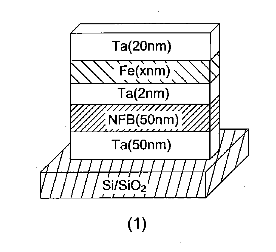
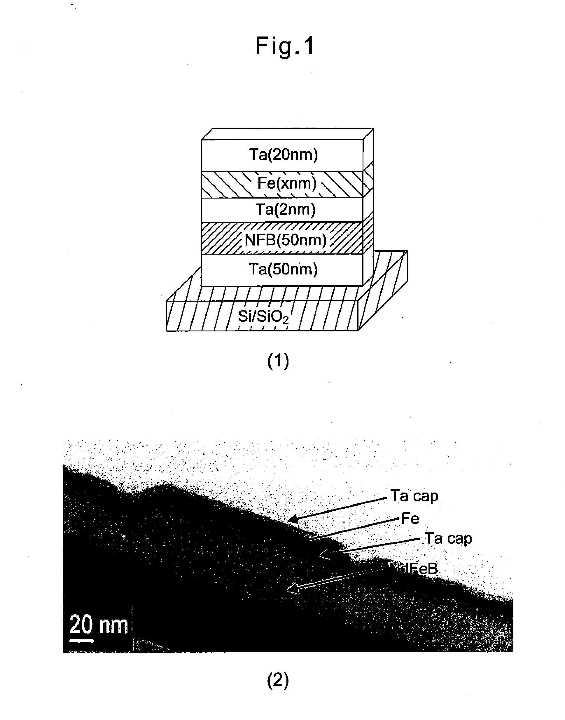
[0030]A film with the structure illustrated schematically in FIG. 1 (1) was formed by sputtering on a thermally-oxidized film (SiO2) of a Si single crystal substrate. The conditions for film forming were as follows. In FIG. 1 (1) “NFB” stands for Nd2Fe14B.
[0031]A) lower Ta layer: formed at room temperature
[0032]B) Nd2Fe14B layer: film formation at 550° C.+annealing at 600° C. for 30 min
[0033]C) Ta spacer layer (intercalated layer)+α-Fe layer+Ta cap layer: film formation between 200 to 300° C.
[0034]wherein the Nd2Fe14B layer of B) is a hard magnetic phase, the Ta spacer layer of C) is an intercalated layer between a hard magnetic phase and a soft magnetic phase, and the α-Fe layer of C) is a soft magnetic phase.
[0035]A TEM micrograph of a cross-sectional structure of the obtained nanocomposite magnet is shown in FIG. 1 (2).
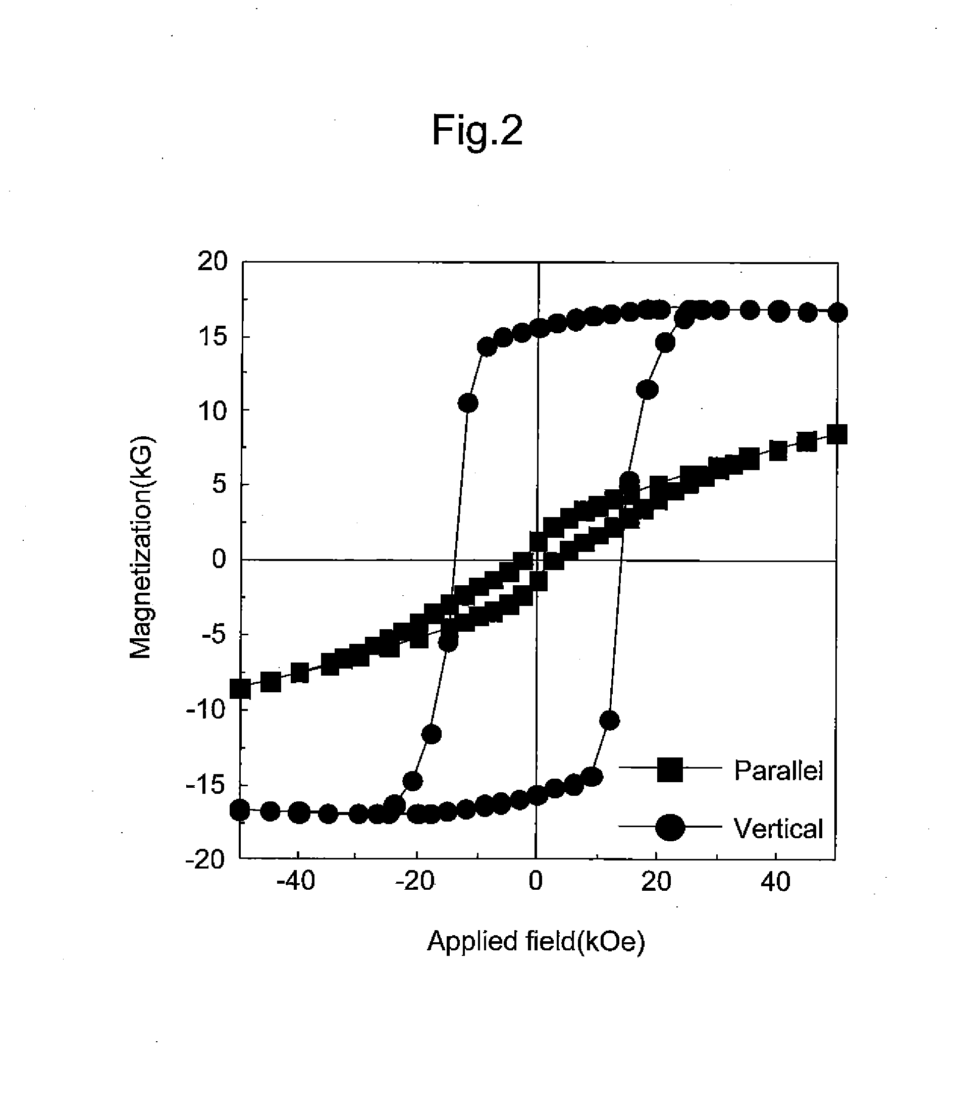
[0036]The magnetization curve of the nanocomposite magnet produced in the current Example is shown in FIG. 2.
[0037]The directions of an applied magnetic field are ...
example 2
[0039]A film with the structure illustrated schematically in FIG. 3 (1) was formed by sputtering on a thermally-oxidized film (SiO2) of a Si single crystal substrate. The conditions for film forming were as follows. In FIG. 3 (1) “NFB” stands for Nd2Fe14B.
[0040]A) lower Ta layer: formed at room temperature
[0041]B′) Nd2Fe14B layer+Nd layer: film formation at 550° C.+annealing at 600° C. for 30 min
[0042]C) Ta spacer layer (intercalated layer)+α-Fe layer+Ta cap layer: film formation between 200 to 300° C.
[0043]wherein the Nd2Fe14B layer of B′) is a hard magnetic phase, the Ta spacer layer of C) is an intercalated layer between a hard magnetic phase and a soft magnetic phase, and the α-Fe layer of C) is a soft magnetic phase.
[0044]The Nd layer formed on the Nd2Fe14B layer was diffused and infiltrated into a grain boundary phase of a Nd2Fe14B phase during annealing.
[0045]A TEM micrograph of a cross-sectional structure of the obtained nanocomposite magnet is shown in FIG. 3 (2).
[0046]The ...
example 3
[0050]A film with the structure illustrated schematically in FIG. 5 was formed by sputtering on a thermally-oxidized film (SiO2) of a Si single crystal substrate. The conditions for film forming were as follows. In FIG. 5“HM” stands for Nd2Fe14B layer (30 nm)+Nd layer (3 nm).
[0051]A) lower Ta layer: formed at room temperature
[0052]B′) Nd2Fe14B layer+Nd layer: film formation at 550° C.+annealing at 600° C. for 30 min
[0053]C) Ta spacer layer+Fe2Co layer+Ta cap layer: film formation between 200 to 300° C.
[0054]wherein the Nd2Fe14B layer of B) is a hard magnetic phase, the Ta spacer layer of C) is an intercalated layer between a hard magnetic phase and a soft magnetic phase, and the Fe2Co layer of C) is a soft magnetic phase.
[0055]As illustrated in FIG. 5, in the 1st cycle, the above A)+B′)+C) were conducted, then in the 2nd to 14th cycles B′)+C) were repeated, and in the 15th cycle B′)+film formation of Ta cap layer were conducted. In other words, 15 HM layers (=Nd2Fe14B layer+Nd layer...
PUM
| Property | Measurement | Unit |
|---|---|---|
| Thickness | aaaaa | aaaaa |
| Thickness | aaaaa | aaaaa |
| Magnetism | aaaaa | aaaaa |
Abstract
Description
Claims
Application Information


