Bjt drive scheme

a drive scheme and switch mode technology, applied in the direction of power conversion systems, dc-dc conversion, instruments, etc., can solve the problems of increasing power consumption, power converter failure to start, comparatively large reservoir of charge needed, etc., to reduce component count and/or cost, improve power efficiency, and reduce the saturation of bipolar transistors

Inactive Publication Date: 2015-01-15
POWER INTEGRATIONS INC
View PDF7 Cites 19 Cited by
  • Summary
  • Abstract
  • Description
  • Claims
  • Application Information

AI Technical Summary

Benefits of technology

[0028]An embodiment may be provided using a switching control circuit IC having the supplementary base drive switch coupled to a supplementary base drive pin on the IC, this preferably lowering component count and / or cost.
[0029]Similarly as for an embodiment of the first aspect, an embodiment optimised operation with regard to switching behaviour of the primary transistor may be achieved. Preferably, the base current switch and supplementary base drive switch turn on and off simultaneously, i.e., their switching instants are substantially (e.g., exactly) coincident. In this case, timing of controlling switching on / off of the base current switch to drive the bipolar transistor does not need to be altered with regard to, e.g., reducing saturation of the bipolar transistor and / or improving power efficiency (such timing preferably based on monitoring for example using comparison to a target turn-off and / or turn-on time of the bipolar transistor). A method of controlling timing of switching the base current switch may simply be extended to control the supplementary base drive switch in preferably perfect synchronism.
[0030]Further advantageously, an embodiment may control voltage on the auxiliary power rail preferably such that the voltage does not exceed a desired maximum, e.g., a maximum supply voltage rating of the switching control circuit. Thus, there may for example be provided the method comprising: controlling the bipolar transistor off throughout an off time period; and driving the supplementary base drive switch on for at least part of the off time period, to allow current flow from the auxiliary power rail through the supplementary base current resistor to thereby reduce voltage on the auxiliary power rail.

Problems solved by technology

However, a bipolar junction transistor generally requires a relatively high drive current and this may give rise to disadvantages for example in relation to power dissipation.
A further disadvantage suffered by the BJT when compared to a voltage-controlled MOSFET, IGBT, etc., is the comparatively large reservoir of charge needed during the start-up procedure.
If the initialisation charge in CAux does not power the IC and BJT for long enough to raise the bias winding voltage to its operational level, the power converter will fail to start.
Loads having a high input capacitance are a particular challenge, as they present an effective short circuit in a ‘cold start’ situation; more switching cycles are therefore required to raise the output and bias winding voltages.
A larger reservoir capacitance requires a higher start-up current, which can increase power consumption.
However it also increases power consumption due to dissipation losses.
Other operating conditions may similarly raise technical issues.
The bias winding voltage is generally closely related to the converter output voltage, so when the output voltage is low there may be insufficient controller IC bias power.
This may occur, for converters operating in constant current or constant power output modes, when a low impedance load causes the output voltage to drop.
Although this problem does occur for MOSFET-based converters, the large current required by a BJT exacerbates it considerably.
Regardless, the external part / whole of the series circuit may shift power dissipation away from the packaged circuit.

Method used


Image

  • Bjt drive scheme
  • Bjt drive scheme
  • Bjt drive scheme

Examples


Embodiment Construction

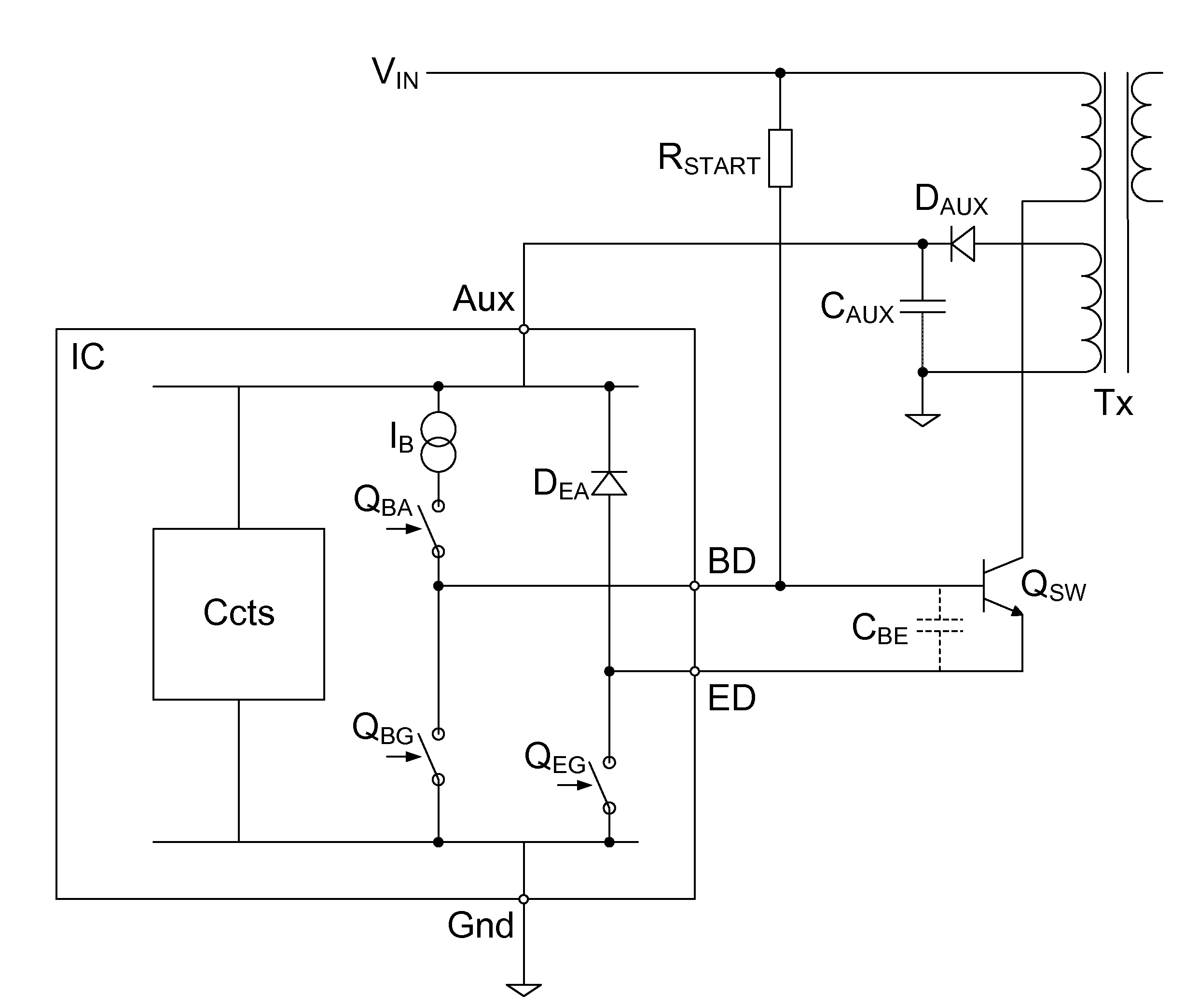
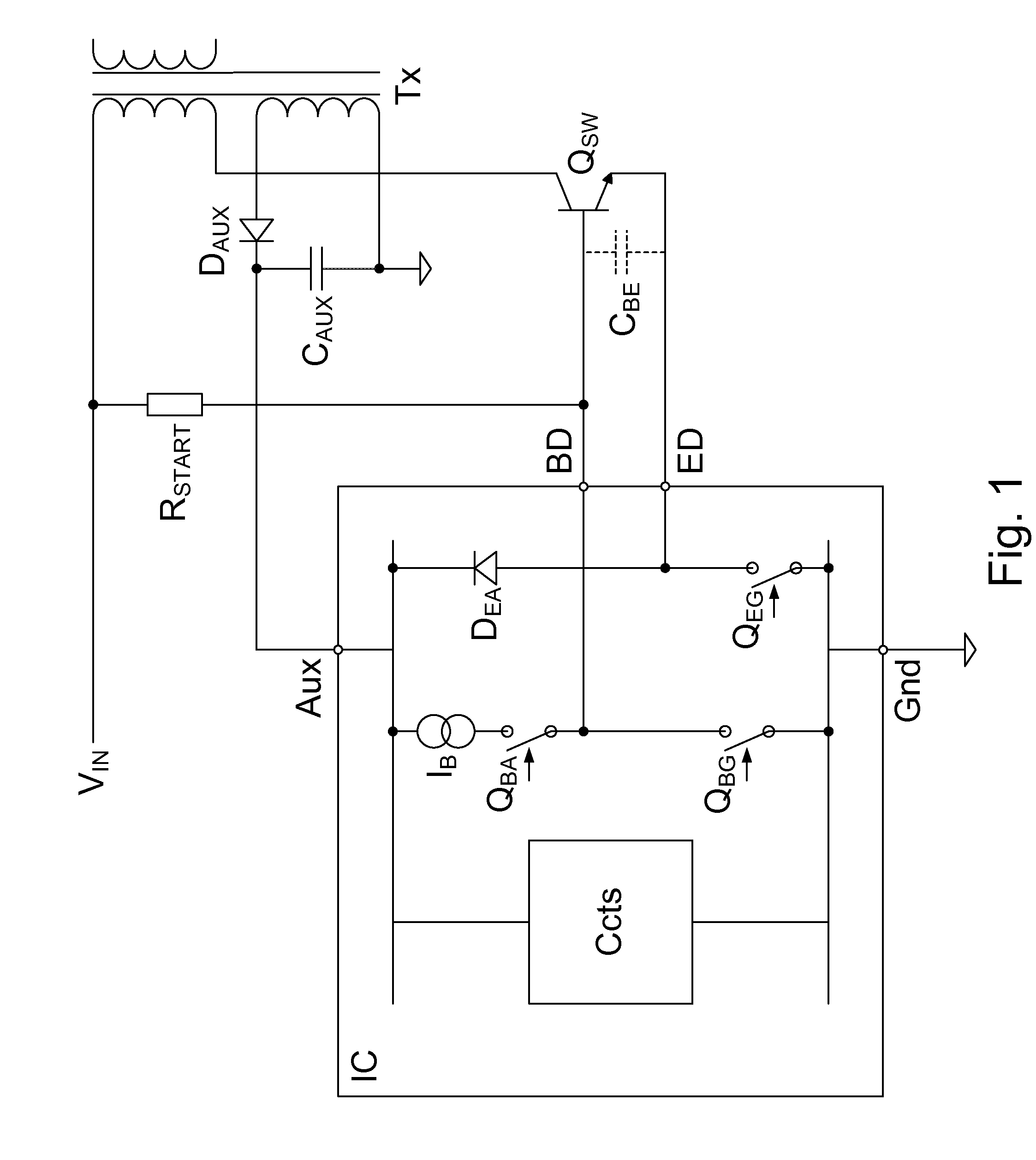
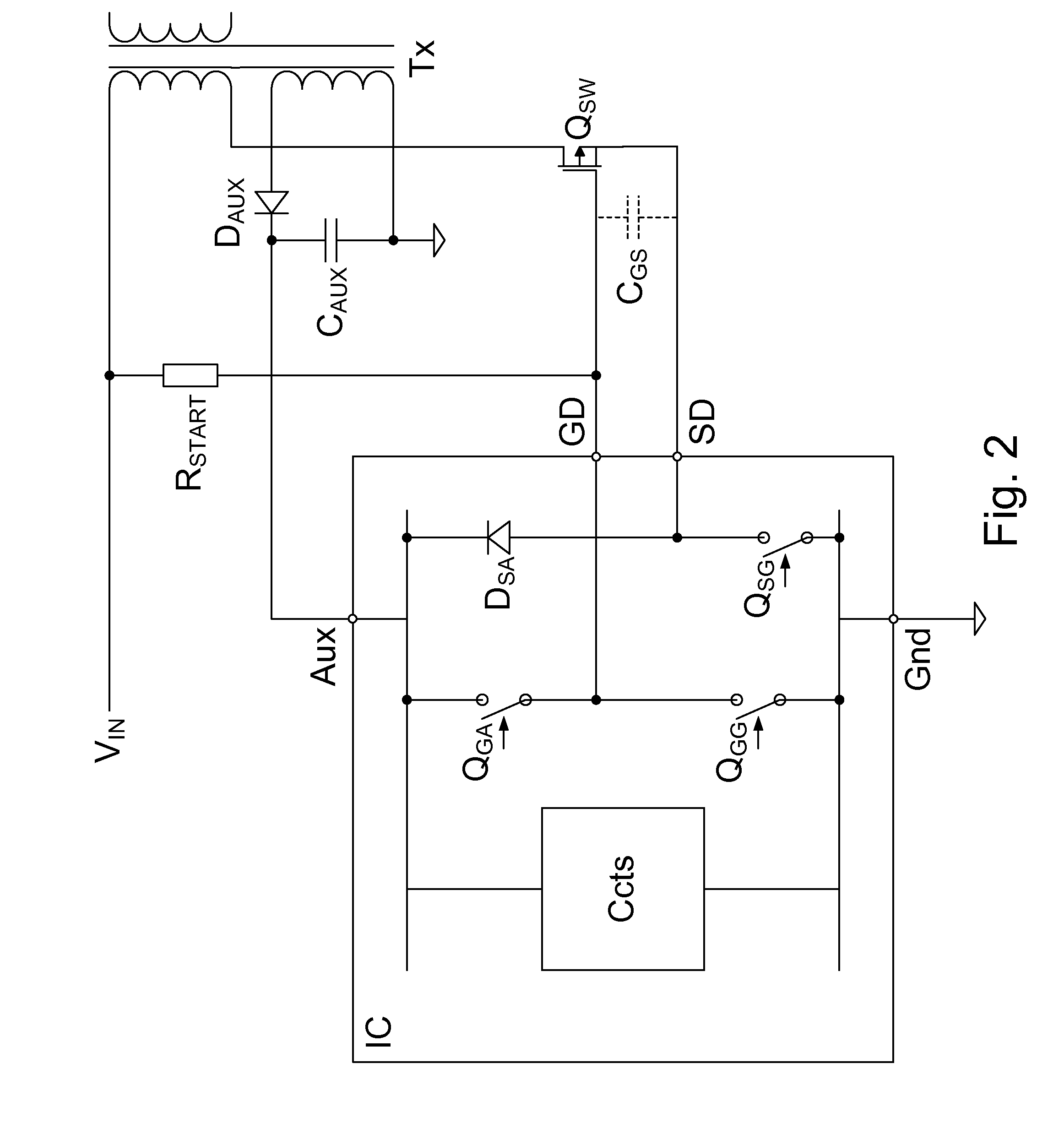
[0049]An embodiment implementing supplementary base drive may allow a controller, which is for controlling switching of the primary switch of a converter using base and emitter drive for the switch control, to be used in higher power rating converters and / or with a lower gain primary switch. To reduce power dissipation in the controller IC, the embodiment supports base current from the auxiliary power circuit via a series circuit (e.g., resistor and diode connection) to supply supplementary base current from the auxiliary rail to the primary switch.

[0050]In a preferred embodiment, the series circuit may have a supplementary base drive (SBD) switch in the series circuit, the switch preferably inside and coupled to an external pin of a switching control circuit package. This SBD switch may be controlled to only turn on when the primary switch is being driven on (in a ‘Chg’ period). In an embodiment, a resistor of the series circuit, which resistor is external to the controller IC, may...


PUM


Abstract

The invention generally relates to switch mode power converters (SMPCs). and methods for providing supplementary base drive to a bipolar transistor of an SMPC, and more particularly to a switching control circuit for a SMPC, a said SMPC having an inductive component coupled to receive power from an input to the SMPC, a bipolar transistor coupled to control current flow in the inductive component, an auxiliary power rail, a charge store for supplying power via the auxiliary rail to a switching control circuit for driving the bipolar transistor, and a bootstrap circuit for bleeding current from the input to the bipolar transistor to thereby provide an amplified current to the charge store, the switching control circuit comprising: a base current line for coupling to a base terminal of a said bipolar transistor, an emitter current line for coupling to an emitter terminal of a said bipolar transistor, an auxiliary line for coupling to a said auxiliary power rail, and at least one reference line for coupling to a reference voltage; a base current switch configured to controllably couple a base current source to the base current line; an emitter current switch configured to controllably couple the emitter current line to a said reference line; a bootstrap element for bleeding current from the emitter current line to the auxiliary line, the bootstrap element further operable to block a said current according to a current or voltage bias; a base discharge switch configured to controllably bleed current from the base current line to a said reference line; and a supplementary base drive line for coupling to a series circuit comprising a supplementary base drive resistor and current control element coupled in series, a said series circuit for bleeding current from a said input to a said base terminal, a said current control element for blocking current flow from a said bootstrap circuit to a said supplementary base drive resistor.

Description

RELATED APPLICATIONS[0001]This application is a continuation-in-part of U.S. application Ser. No. 14 / 184,073, filed Feb. 19, 2014, which application claims priority under 35 U.S.C. §119(e) to U.S. Provisional Application No. 61 / 767,023, filed Feb. 20, 2013; and to U.S. Provisional Application No. 61 / 888,778, filed Oct. 9, 2013, which applications are incorporated herein by reference in their entirety.FIELD OF THE INVENTION[0002]The present invention generally relates to switch mode power converters (SMPCs) and methods for providing supplementary base drive to a bipolar transistor of an SMPC, and more particularly to a switching control circuit for a SMPC.BACKGROUND TO THE INVENTION[0003]The use of a low cost bipolar junction transistor (BJT) for the primary switch in an offline power converter is desirable, since it provides both high breakdown voltage and low on-state voltage. However, a bipolar junction transistor generally requires a relatively high drive current and this may giv...

Claims


Application Information

Patent Timeline
Patent Type & Authority Applications(United States)
IPC IPC(8): H02M1/08H02M1/36
CPCH02M1/08H02M1/36H02M3/156H02M3/335H02M1/0006
Inventor BHASIN, MANOJWERNER, ANTONIUS JACOBUS JOHANNESRYAN, PAULPIPER, JOHAN
Owner POWER INTEGRATIONS INC
Why Eureka
Try Eureka