Method of using non-volatile memories for on-dimm memory address list storage

a non-volatile memory and address list technology, applied in static storage, digital storage, instruments, etc., can solve the problems of inability to reliably retain information at certain address locations, degrade the reliability of dram cells, etc., to facilitate the “repair” and improve memory performance. , the effect of improving performance and lifetim

Active Publication Date: 2015-01-15
RAMBUS INC
View PDF2 Cites 4 Cited by
  • Summary
  • Abstract
  • Description
  • Claims
  • Application Information

AI Technical Summary

Benefits of technology

[0018]Many benefits are achieved by way of the present invention over conventional embodiments and techniques. For example, embodiments of a memory integrated circuit device can have improved performance and lifetime. Embodiments of a memory interface device can facilitate the “repair” of bad or faulty memory cells, or even undesirable memory cells due to aging, deterioration, or the like. Spare memory cells from a memory IC device can be rerouted via a memory interface device upon detection of predetermined characteristics of memory cell to be replaced. These implementations provide several means of maintaining or improving memory performance, which can be tailored depending on various hardware and / or software requirements of specific applications. Additional benefit lies in an implementation of array of spare memory cells dedicated for a plurality of DRAM memory devices to eliminate inefficient spare rows and / or columns of cells. An integrated circuit device includes a match table using non-volatile memory to store the address-list information from the plurality of DRAM memory devices and use a controller built in a SRAM device to process and determine the address of bad cell and output information of replacing the bad address by a revised address in the dedicated spare memory cells. Specifically, a dual-purpose pin is used to applied high voltage required for non-volatile programming without need for a charge pump to save device real estate. At least this is able to handle a minimized single-bit or very small number of bits at a time to store the address-list information to the non-volatile memory. Also, in-field non-volatile memory update is possible with this integrated circuit device.

Problems solved by technology

As DRAM technologies scale to higher and higher density with smaller and smaller feature sizes, the reliability of DRAM cells degrade and certain address locations will not be able to retain information reliably.

Method used


Image

  • Method of using non-volatile memories for on-dimm memory address list storage
  • Method of using non-volatile memories for on-dimm memory address list storage
  • Method of using non-volatile memories for on-dimm memory address list storage

Examples


Embodiment Construction

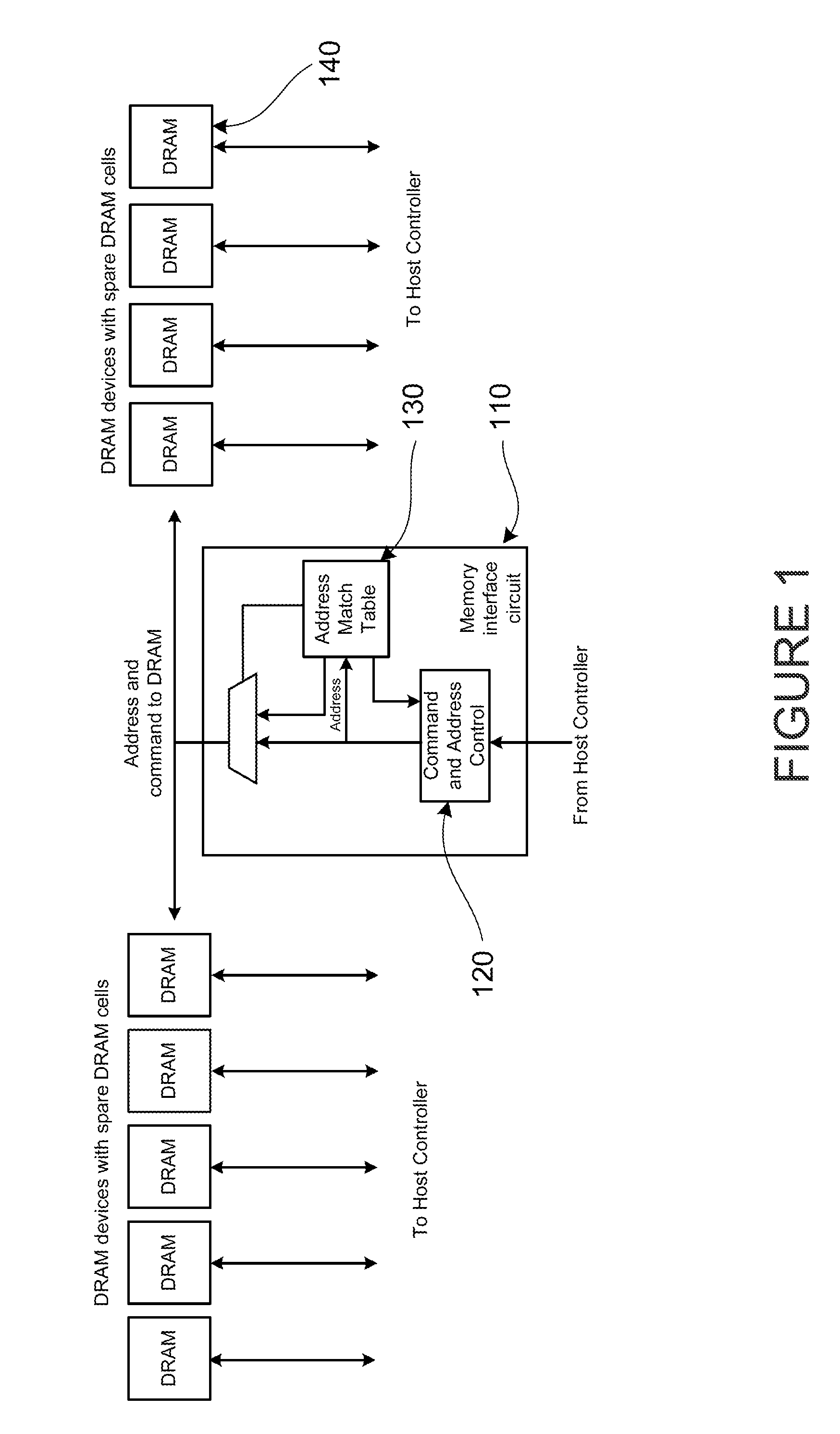
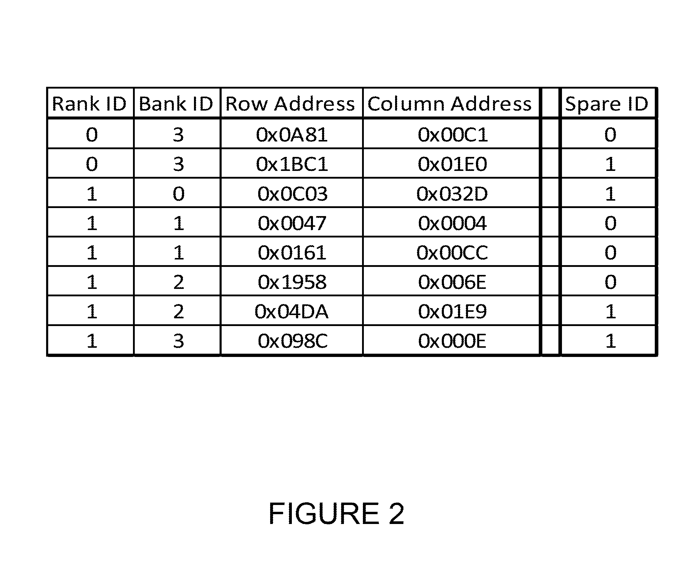
[0037]Certain DRAM memory cells are turned to bad cells or weak cells because of its charge level from programming is not stable. Therefore, bad cell repair operation becomes desirable. In a conventional way, DRAM memory chip includes one or more spare rows and / or columns of cells for being used to replace a cell that is determined to be defective. However, this approach may require that an entire spare row or column be used to repair a single bit, which is done in very poor efficiency.

[0038]Therefore, new techniques for replacing the defective cell in DRAM chip with much improved efficiency are desired. For example, a random repair method may be implemented to use logic for randomly addressing any of spare memory cells without need the use of an entire row or column of spare cells to replace a single defective cell. Advanced DRAM devices such as SDRAM or DIMM devices can be provided within an integrated memory chip without requiring allocation of those spare rows or columns, recove...


PUM


Abstract

An integrated circuit device. The device includes an address input(s) configured to receive address information from an address stream from an address command bus coupled to a host controller and an address output(s) configured to drive address information, and is coupled to a plurality of memory (DRAM) devices provided on a DIMM. The device has an address match table comprising a non-volatile memory device configured to store at least a revised address corresponding to a spare memory location and a bad address of at least one of the plurality of memory (DRAM) devices. The device has a control module configured to process and determine whether each address matches with a stored address in the address match table to identify the bad address and configured to replace the bad address with the revised address of the spare memory location.

Description

CROSS-REFERENCES TO RELATED APPLICATIONS[0001]The present application is a continuation of and claims priority to U.S. patent application Ser. No. 13 / 791,814 filed Mar. 8, 2013, which claims priority of and incorporates by reference, for all purposes, U.S. Provisional Patent Application No. 61 / 664,304 filed Jun. 26, 2012, commonly assigned.BACKGROUND OF THE DISCLOSURE[0002]The present invention relates generally to solid state memory techniques. More particularly, the present invention provides methods and devices for storing memory cell address list with identified “bad memory cell” in a non-volatile memory device for repairing the bad cell in a dynamic random access memory (“DRAM”) device or others.[0003]DRAM continues to be widely used in laptop and workstation computers as well as some of the RAM of video game consoles simply due to its structural simplicity and high density. As DRAM technologies scale to higher and higher density with smaller and smaller feature sizes, the reli...

Claims


Application Information

Patent Timeline
Patent Type & Authority Applications(United States)
IPC IPC(8): G11C29/04G11C11/413G11C16/08G11C7/10
CPCG11C7/1012G11C16/08G11C11/413G11C29/04G11C5/04G11C29/08G11C29/44G11C2029/4402G11C29/76G11C29/785G11C8/06
Inventor RATEGH, HAMID REZAWANG, DAVID T.TSE, LAWRENCE
Owner RAMBUS INC
Why Eureka
Try Eureka