Electric power source device

a technology of power source device and power supply device, which is applied in the direction of process and machine control, association of printed circuit non-printed electric components, instruments, etc., can solve the problems of unusable space around the components, and achieve the effect of effectively using such unusable spa

Active Publication Date: 2015-01-29
DENSO CORP
View PDF4 Cites 12 Cited by
  • Summary
  • Abstract
  • Description
  • Claims
  • Application Information

AI Technical Summary

Benefits of technology

[0007]It is therefore desired to provide an electric power source device having an improved structure capable of effectively utilizing an overall space formed on a mounting surface of a base plate and easily reducing an overall size of the electric power source device.
[0009]The electric power source device has one or more the stacked sections. In each of the stacked sections, two components selected from the primary side semiconductor components, the secondary side semiconductor components, and a combination of the transformer and the secondary side semiconductor components are stacked. The stacked section is mounted on the mounting surface of the base plate and arranged in the direction of the normal line of the mounting surface of the base plate. Further, at least a part of the substrate side electrical components is arranged inside of an exterior part of the component having the maximum exterior size forming the stacked section in the horizontal direction. The horizontal direction is perpendicular to the direction of the normal line of the mounting surface of the base plate. Still further, this part of the substrate side electrical components is arranged inside of the second surface of the stacked section toward the mounting surface side in the vertical direction. The second surface of the stacked section is opposing to the first surface of the stacked section. The first surface of the stacked section is directly in contact with the mounting surface of the base plate when viewed along the vertical direction which is parallel to the direction of the normal line of the mounting surface. This structure makes it possible to provide effective use for the space generated around the stacked section in the inside of the electric power source device.
[0010]That is, the stacked section has a structure in which at least two components having a different exterior size are stacked in the direction of the normal line of the mounting surface of the base plate. Accordingly, an unusable space is formed in the space adjacent to the component having a small exterior size in the horizontal direction which is perpendicular to the stacking direction of the stacked section, i.e. in the direction of the normal line of the mounting surface of the base plate. On the other hand, in particular, in the improved structure of the electric power source device according to the present invention, the substrate-side electrical component mounted on the circuit substrate is arranged in the unusable area formed in the space around, i.e. adjacent to the component having a small exterior size in the stacked section in the horizontal direction. This makes it possible to provide the miniaturized electric power source device because of effectively using such unusable space.

Problems solved by technology

However, the conventional technique disclosed in the patent document described above may cause the following problem.
This often generates an unusable space around the components having a small exterior size when the components are stacked on the mounting surface of the base plate in order to make a stacked section.

Method used


Image

  • Electric power source device
  • Electric power source device
  • Electric power source device

Examples


first exemplary embodiment

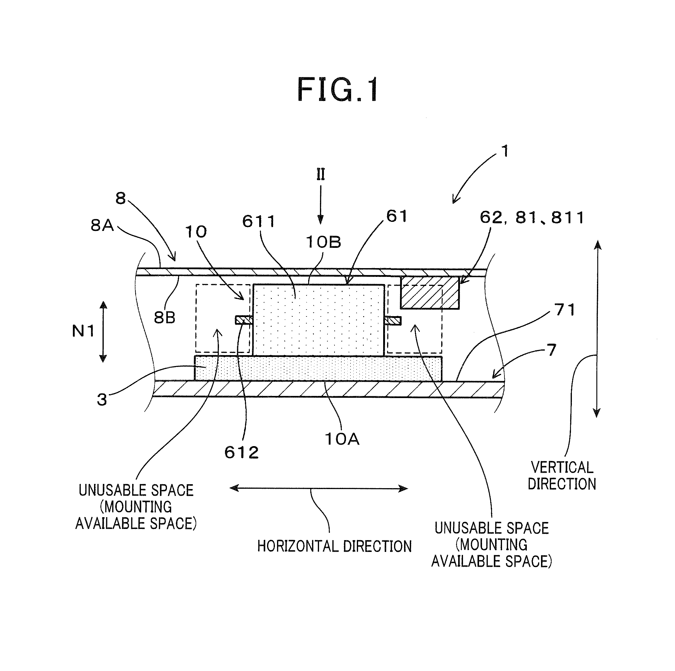
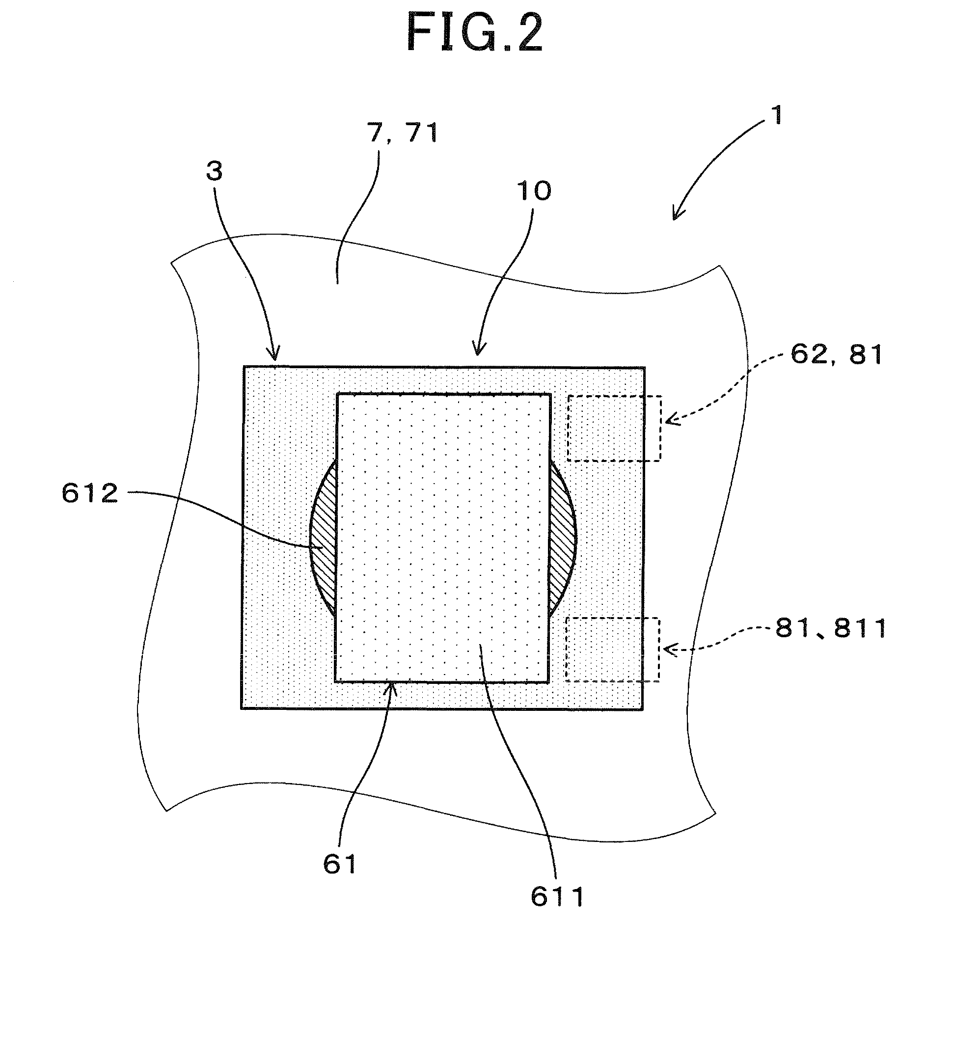
[0032]A description will now be given of an electric power source device 1 according to the first exemplary embodiment with reference to FIG. 1, FIG. 2 and FIG. 3.

[0033]FIG. 1 is an explanatory view showing the electric power source device 1 according to the first exemplary embodiment. FIG. 2 is a view showing the structure of the electric power source device 1 in a section taken along the line II shown in FIG. 1. FIG. 3 is a view showing a circuit structure of the electric power source device 1 according to the first exemplary embodiment shown in FIG. 1.

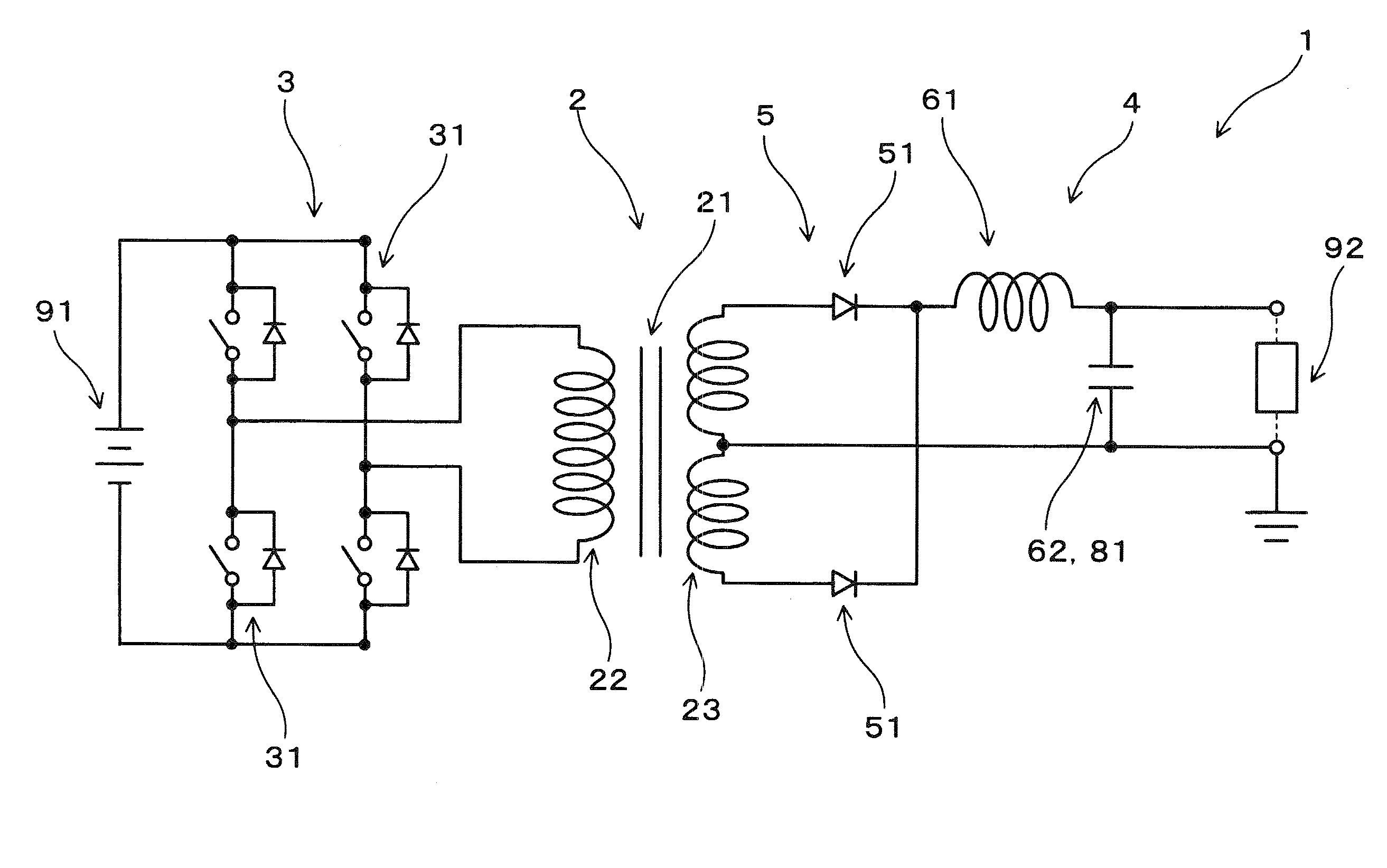
[0034]As shown in FIG. 1, FIG. 2 and FIG. 3, the electric power source device 1 according to the first exemplary embodiment is comprised of a transformer 2, a primary side semiconductor module 3, a secondary side semiconductor module 5, a choke coil 61, a base plate 7 and a circuit substrate 8.

[0035]The primary side semiconductor module 3 is a primary side semiconductor component which is connected to the transformer 2. The secondar...

second exemplary embodiment

[0059]A description will be given of the electric power source device 1 according to the second exemplary embodiment with reference to FIG. 4 and FIG. 5.

[0060]FIG. 4 is an explanatory view showing a structure of the electric power source device 1 according to the second exemplary embodiment. FIG. 5 is a sectional view showing the structure of the electric power source device 1 taken along the line V shown in FIG. 4.

[0061]As shown in FIG. 4 and FIG. 5, the circuit substrate 8 is arranged so that the direction of a normal line N2 of the circuit substrate 8 becomes perpendicular to the direction of the normal line N2 of the base plate 7. That is, the direction of the normal line N2 is a horizontal line in FIG. 4 and the direction of the normal line N1 is a vertical line in FIG. 4. Accordingly, the circuit substrate 8 is arranged at the right side on the mounting surface 71 of the base plate 7 along the direction of the normal line N1 of the base plate 7.

[0062]As clearly shown in FIG. 4...

third exemplary embodiment

[0064]A description will be given of the electric power source device 1 according to the third exemplary embodiment with reference to FIG. 6 and FIG. 7.

[0065]FIG. 6 is an explanatory view showing a structure of an electric power source device according to the third exemplary embodiment. FIG. 7 is a sectional view showing the structure of the electric power source device taken along the line VII shown in FIG. 6. The electric power source device 1 according to the third exemplary embodiment shown in FIG. 6 and FIG. 7 is different in a part of the structure from the electric power source device 1 according to the second exemplary embodiment shown in FIG. 4 and FIG. 5.

[0066]The stacked section 10 of the electric power source device 1 according to the third exemplary embodiment has the structure in which a center line C1 of the primary side semiconductor module 3 is shifted from a center line C2 of the choke coil 61 by a predetermined length when viewed along the direction of the normal ...


PUM


Abstract

An electric power source device has a transformer, a primary-side semiconductor module, a secondary-side semiconductor module, a secondary-side electrical component, a base plate and a circuit substrate on which substrate-side electrical components are mounted. The primary-side semiconductor module has a larger exterior size than the secondary-side electrical component. The primary-side semiconductor module and the secondary-side electrical component form a stacked section. In the stacked section, the secondary-side electrical component is stacked, in a vertical direction, i.e. a direction of a normal line of a mounting surface of the base plate, on the primary-side semiconductor module. The primary-side semiconductor module is directly mounted on the mounting surface. At least a part of the substrate-side electrical components is arranged inside of the primary-side semiconductor module in a horizontal direction, and inside of a second surface of the stacked section toward the mounting surface along the normal line.

Description

CROSS-REFERENCE TO RELATED APPLICATION[0001]This application is related to and claims priority from Japanese Patent Applications No. 2013-153638 filed on Jul. 24, 2013, and 2014-88981 filed on Apr. 23, 2014, the contents of which are hereby incorporated by reference.BACKGROUND OF THE INVENTION[0002]1. Field of the Invention[0003]This present invention relates to electric power source devices to be used in hybrid vehicles, electric vehicles etc.[0004]2. Description of the Related Art[0005]Hybrid vehicles and electric vehicles usually use electric power source devices such as charging devices and direct current to direct current (DC-DC) converters. Such a charging device is usually equipped with the DC-DC converter. For example, a patent document Japanese patent laid open publication No. 2012-213309 has disclosed a conventional electric power source device. The electric power source device is generally comprised of a transformer, semiconductor elements, a smoothing circuit and a base ...

Claims


Application Information

Patent Timeline
Patent Type & Authority Applications(United States)
IPC IPC(8): H02M3/335
CPCH02M3/33507H05K1/0263H05K1/18H05K2201/1003H05K2201/10166H05K2201/10174H05K2201/10515B60L15/007B60L2210/10Y02T10/64Y02T10/72H02M3/003H02M3/33573H01F5/00
Inventor TAKEMOTO, YUUKIMISAWA, KATSUTOYOHANDA, YUUICHIYAMASAKI, SYOTAROUKURAUCHI, SYUJIHATAKENAKA, KENTA
Owner DENSO CORP
Why Eureka
Try Eureka