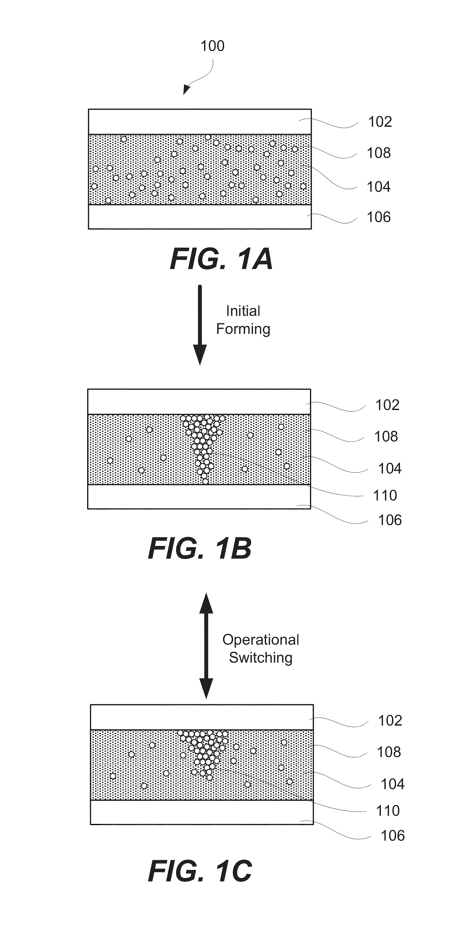
It is believed that various defects change their location forming the conductive paths (when the set
voltage is applied) and breaking the conductive paths (when the reset
voltage is applied) and causing changes in the resistance.
This change in orientation causes formation of the conductive paths or breaking of the conductive paths, which results in changes of the resistance.
Some materials or vacancies may not be sufficiently mobile, while mobility of other materials or vacancies may not
impact the resistance.
Having multiple types of defects operating simultaneously within the switching zone may interfere with
resistive switching characteristics and may be difficult, if possible at all to control.
In other words, if the switching zone does not have enough defects, then the conductive paths may be hard to form if these paths can be formed at all.
On the other hand, if the switching zone has too many defects, then the conductive paths may be difficult to break as there are many conductive paths capable of conductive
electrical current and larger overall power may be required.
Precisely controlling distribution of defects in such
thin layer is challenging.
While these other portions may exhibit some defect mobility, the change in resistance caused by this mobility is negligible because of relatively
high concentration of defects.
It should be noted however that some of these other components may still include defects, but these defects are relative immobile in these components.
The challenge in controlling distribution of defects within ReRAM cells is due to very thin
layers used for these cells.
Furthermore, ReRAM cells are often subject to high temperatures, e.g., used for annealing and activating other components, such as diodes.
Materials in thin films (e.g., less 50 Angstroms) readily intermix when exposed to high temperatures that may result in uniform distribution of defect and difficulties in defining a switching zone.
The gradual distribution of defects does not provide a similar switching effect and result in generally high switching voltages.
Very few materials are effective blockers of metals when subjected to annealing and resistive switching conditions.
Without boundary for defect movement, there is very little control that can be exerted on defect distribution.
In fact, in some embodiments, the defect blocking layer may release some defects into the defects acceptor layer.
While this modified layer now containing
aluminum oxynitride can be used as a resistive switching layer, the distribution of
nitrogen within the layer is gradual and will become even more gradual with subsequent annealing, which is not desirable.
Furthermore, controlling the amount of
nitrogen introduced into this layer may be difficult.
That is, defects may travel through an interface formed by this
electrode with the resistive switching layer (i.e., the reactive interface).
Furthermore, there may be some mobility of defects within resistive switching layer 104.
This breakage generally does not correspond to complete dispersion of defects forming these conductive paths and may be a self-limiting process, i.e., the process may stop after some initial breakage occurs.
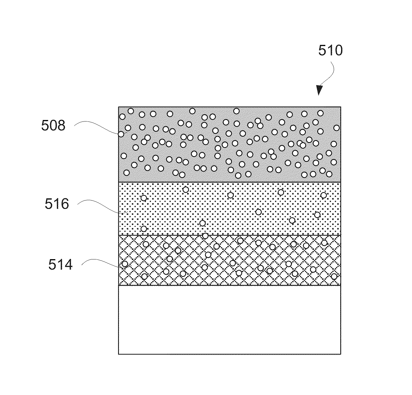
Furthermore, inherently unstable materials, such as oxides having multiple phases, may be used to form defect source layer 304.
This commonality of materials may be used to avoid transfer of these materials between
layers and creating additional uncontrollable defects that may
skew the resistive switching performance.
As such, the transfer may be limited to defects.
However, while defect acceptor layer 306 is capable of accepting defects from defect source layer 304, defect blocking layer 308 is not capable of accepting defects from defect acceptor layer 306.
In some embodiments, defects may be introduced into the defect source layer during its deposition.
However, mobility of defects within the defect blocking layer and the defect source layer may be different.
Without being restricted to any particular theory, it is believed that combining
layers having different compositions (e.g., aluminum
oxide and aluminum
nitride) into a nano-laminate will create an unstable layer.
The fact that
nitrogen concentration 702 tapers down within doped polysilicon
electrode is irrelevant since nitrogen is not capable of sufficiently
impact resistance of this layer

