Local seal for encapsulation of electro-optical element on a flexible substrate

a technology of electro-optical elements and local seals, which is applied in the direction of thermoelectric device junction materials, semiconductor devices, electrical apparatus, etc., can solve the problems of limited heat tolerance, limited tolerance of optical elements, and limited heat toleran

Active Publication Date: 2015-02-05
GLOBAL OLED TECH
View PDF16 Cites 13 Cited by
  • Summary
  • Abstract
  • Description
  • Claims
  • Application Information

AI Technical Summary

Benefits of technology

[0041]In a sixteenth aspect of the present invention, the glass powder suspension is doped with a fluorescent or other color shifting ma

Problems solved by technology

Many of these electro-optical elements contain organic materials and have limited tolerance for heat.
OLED elements are particularly sensitive to moisture, are sensitive to oxygen, and have limited tolerance for heat.
However, as discussed below, encapsulation suitable for flexible products has not been satisfactorily addressed to date, especially for the stringent encapsulation requirements of OLED elements.
A metal substrate is opaque and is only suitable for a bottom-emitting display, while a glass substrate is relatively thick and rigid, and not well-suited for roll-to-roll manufacture or flexible displays.
Thin film enc

Method used


Image

  • Local seal for encapsulation of electro-optical element on a flexible substrate
  • Local seal for encapsulation of electro-optical element on a flexible substrate
  • Local seal for encapsulation of electro-optical element on a flexible substrate

Examples


first embodiment

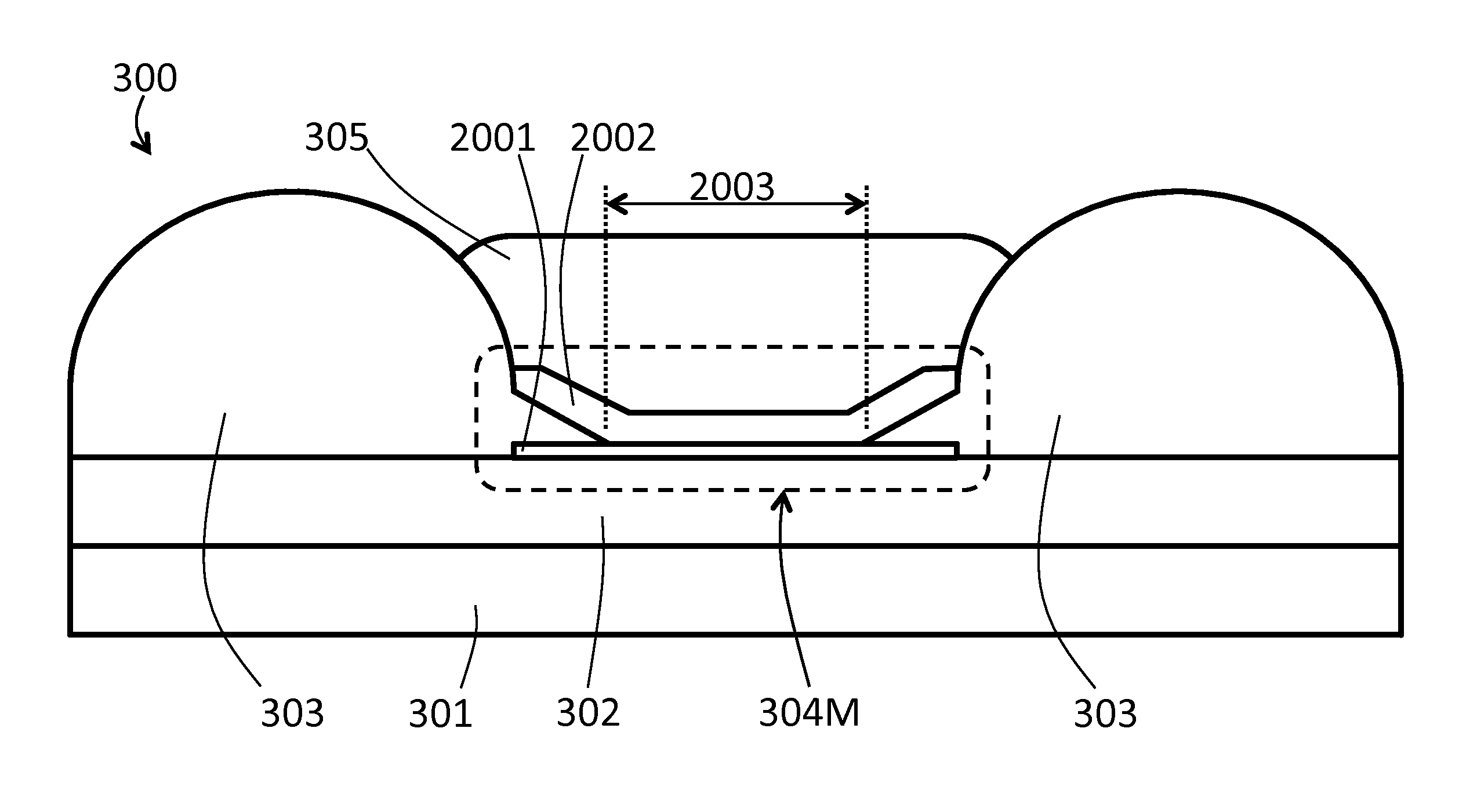
[0078]FIG. 3 depicts the present invention. Panel 300 comprises electro-optical elements 304R, 304G, 304B formed over a lower substrate 301. Electro-optical elements 304R, 304G, 304B are part of a two-dimensional array of electro-optical elements 304 formed over the substrate 301. (Two-dimensional arrays of elements are discussed further, below, in context of FIG. 22.) Above each electro-optical element 304R, 304G, 304B is a respective local seal 305R, 305G, 305B. Between lower substrate 301 and electro-optical elements 304R, 304G, 304B there may be intermediate layers variously including one or more of buffer layers, planarization layers, dielectric layers, banks, passive wiring layers, and active TFT layers: these are collectively represented in FIG. 3 by structure 302.

[0079]Individual electro-optical elements 304R, 304G, 304B are separated by banks 303. The banks 303 may be formed integrally with structure 302 or separately. The banks are shown extending in height above the elect...

second embodiment

[0095]Turning now to FIG. 4A, panel 400 is a preferred second embodiment of a lighting panel comprising light emitting elements separated by banks 303. The lighting panel may be part of a lighting fixture or other lighting product, either as a removable part or as an integrally fabricated component. FIG. 21(f), adapted from U.S. Pat. No. 7,638,941 shows a ceiling-mount OLED chandelier 2160; each OLED panel 2167 is a removable unit.

[0096]Each light emitting element has a respective local seal 405. As shown, the local seals 405 are hexagonal and are arranged in a hexagonal pattern forming a two-dimensional array. Although not visible in this view, it can be inferred that the light emitting elements underneath the local seals 405 are also arranged in a similar hexagonal pattern forming a two-dimensional array. Of course, other patterns are possible. For example, FIG. 21(e), adapted from U.S. Pat. No. 6,870,196, shows an OLED lighting panel 2150 comprising a rectangular array of polygon...

third embodiment

[0103]It is not necessary for each individual electro-optical element or light emitting element to have its own independent local seal in order to realize the benefits of the present invention. FIG. 5 shows a panel 500 wherein local seals 505A, 505B cover respective groups of electro-optical elements 504A, 504B. The individual elements 504A are mutually separated by banks 506, while a group of elements 504A and its associated local seal 505A is separated from a neighboring group of elements 504B and its associated local seal 505B by bank 503. In preferred embodiments, the height of bank 506 is less than the height of bank 503, but this is not necessary. Between lower substrate 301 and elements 504A, 504B lies structure 302, providing the same or similar functions as described above.

[0104]FIG. 18 shows a curved or flexed panel 1800 utilizing local seals 1805 over electro-optical elements (not shown) formed on substrate 1801. Panel 1800 may be part of a display product, a lighting pro...


PUM


Abstract

An electroluminescent display or lighting product incorporates a panel comprising a collection of distinct light-emitting elements formed on a substrate. A plurality of distinct local seals are formed over respective individual light-emitting elements or groups of light-emitting elements. Each local seal is formed by depositing a low melting temperature glass powder suspension or paste using inkjet technology, and fusing the glass powder using a scanning laser beam having a tailored beam profile. The local seal may be used in conjunction with a continuous thin film encapsulation structure. Optical functions can be provided by each local seal, including refraction, filtering, color shifting, and scattering.

Description

CROSS-REFERENCE TO RELATED APPLICATION[0001]This application claims the benefit of U.S. Provisional Application No. 61 / 859,989, filed Jul. 30, 2013.FEDERALLY SPONSORED RESEARCH[0002]Not applicableFIELD OF THE INVENTION[0003]The present invention relates to encapsulation of a flexible electroluminescent device or similar electro-optical panel.BACKGROUND[0004]Electro-optical arrays are widely used in commercial products. Examples of such products include a phone, a monitor, a television set, and a wristwatch, all of which have pixel arrays used for information display. Further examples include an OLED lighting panel and an OLED luminaire, which have arrays of OLED elements used for illumination.[0005]Display Products[0006]In recent years, there has been a blurring of lines between some of the abovementioned product categories. For example, modern smartphones routinely include cameras and allow viewing of video and television received over wireless networks and the Internet. Additional...

Claims


Application Information

Patent Timeline
IPC IPC(8): H01L51/52H01L27/32
CPCH01L27/3244H01L51/524H10K59/122H10K50/854H10K50/858H10K50/844H10K2102/311H10K50/841H10K50/84H10K59/00H10K59/12H10K71/00H10K71/164
Inventor ROHATGI, RAJEEV
Owner GLOBAL OLED TECH
Why Eureka
Try Eureka