Unlock instant, AI-driven research and patent intelligence for your innovation.
Semiconductor package and method of fabricating the same
Inactive Publication Date: 2015-02-05
SILICONWARE PRECISION IND CO LTD
View PDF10 Cites 11 Cited by
Summary
Abstract
Description
Claims
Application Information
AI Technical Summary
This helps you quickly interpret patents by identifying the three key elements:
Problems solved by technology
Method used
Benefits of technology
Benefits of technology
The patent text describes a new semiconductor package and a method of making it that eliminates the need for a traditional silicon interposer, reducing fabrication costs and simplifying the process. This results in higher productivity and yield, making it a better overall solution.
Problems solved by technology
In addition, due to problems associated with thermal stress and warpage as a result of mismatch of heat expansion coefficient between semiconductor chip and substrate, the reliability between the semiconductor chip and the substrate is decreased causing frequent failures in reliability test.
Hence, it is difficult to lower the overall cost.
Moreover, the technical difficulty in fabricating the silicon interposer 10 is high, and hence below the same fabricating cost, the yield of the semiconductor package 1 is relatively low.
Method used
Image
Click on the blue label to locate the original text in one second.
Reading with bidirectional positioning of images and text.
Examples
Embodiment Construction
[0032]The present invention is described in the following with specific embodiments, so that one skilled in the pertinent art can easily understand other advantages and effects of the present invention from the disclosure of the present invention.
[0033]It is to be understood that the scope of the present invention is not limited to the disclosed embodiments. On the contrary, it is intended to cover various modifications and similar arrangements. The scope of the claims, therefore, should be accorded the broadest interpretation so as to encompass all such modifications and similar arrangements. In addition, words such as “on”, “top” and “a” are used to explain the preferred embodiment of the present invention only and should not limit the scope of the present invention.
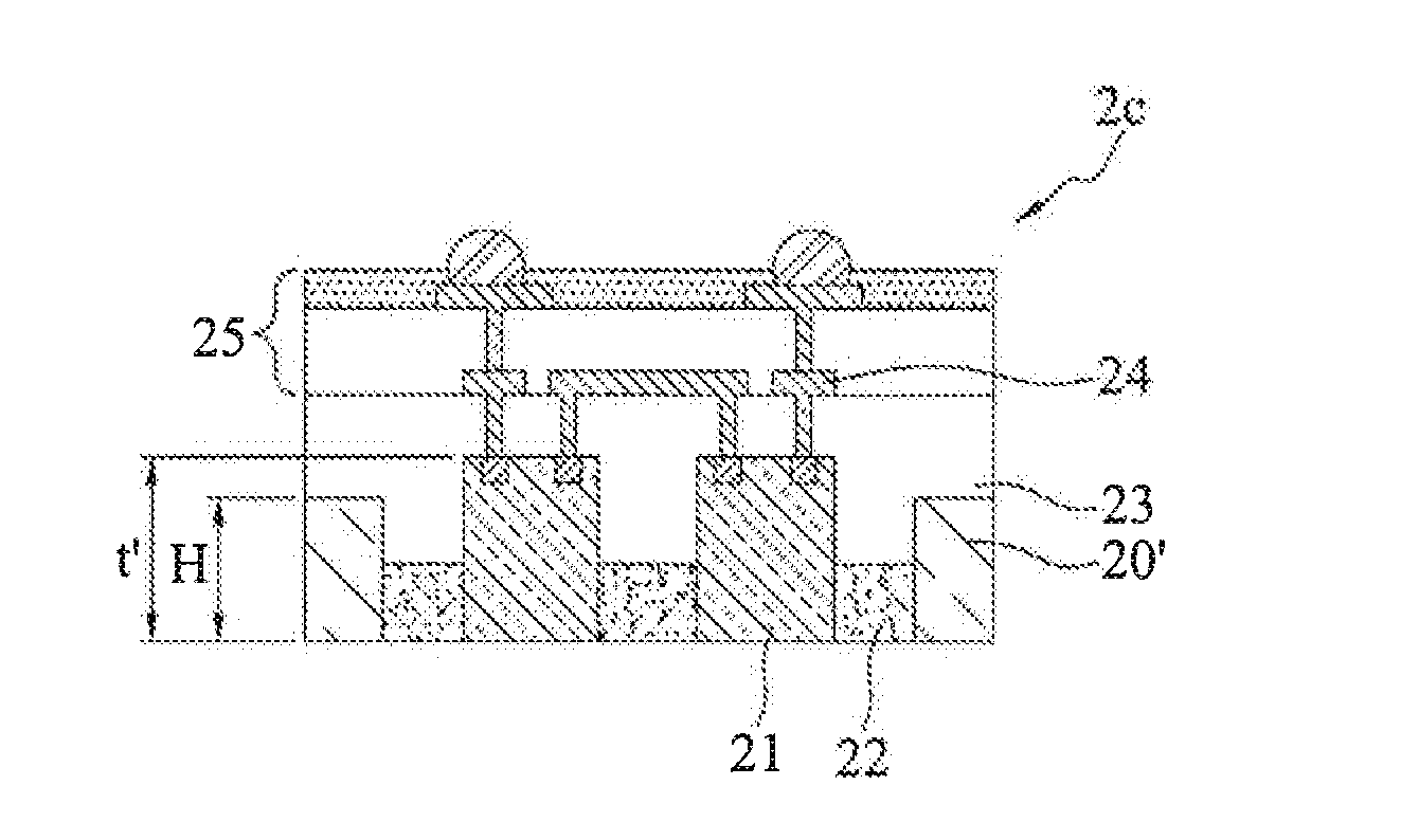
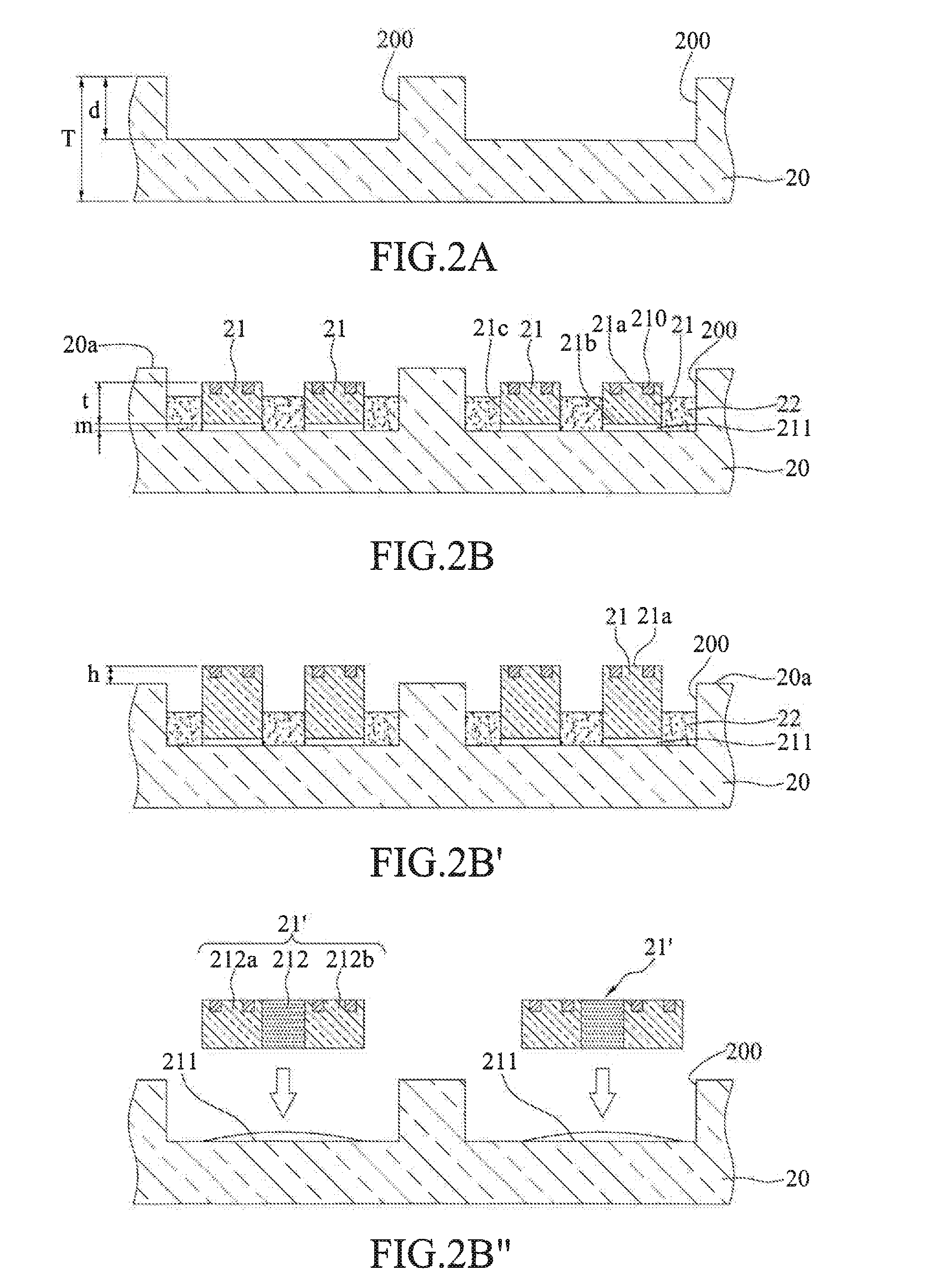
[0034]FIGS. 2A-2H are schematic cross-sectional views showing a method of fabricating a semiconductor package 2a-2f in accordance with a first embodiment of the present invention.
[0035]As shown in FIG. 2A, a carrier 20...
PUM
Abstract
The present invention provides a semiconductorpackage and a method of fabricating the same, including: placing in a groove of a carrier a semiconductor element having opposing active and non-active surfaces, and side surfaces abutting the active surface and the non-active surface; applying an adhesive material in the groove and around a periphery of the side surfaces of the semiconductor element; forming a dielectric layer on the adhesive material and the active surface of the semiconductor element; forming on the dielectric layer a circuit layer electrically connected to the semiconductor element; and removing a first portion of the carrier below the groove to keep a second portion of the carrier on a side wall of the groove intact for the second portion to function as a supporting member. The present invention does not require formation of a siliconinterposer, and therefore the overall cost of a final product is much reduced.
Description
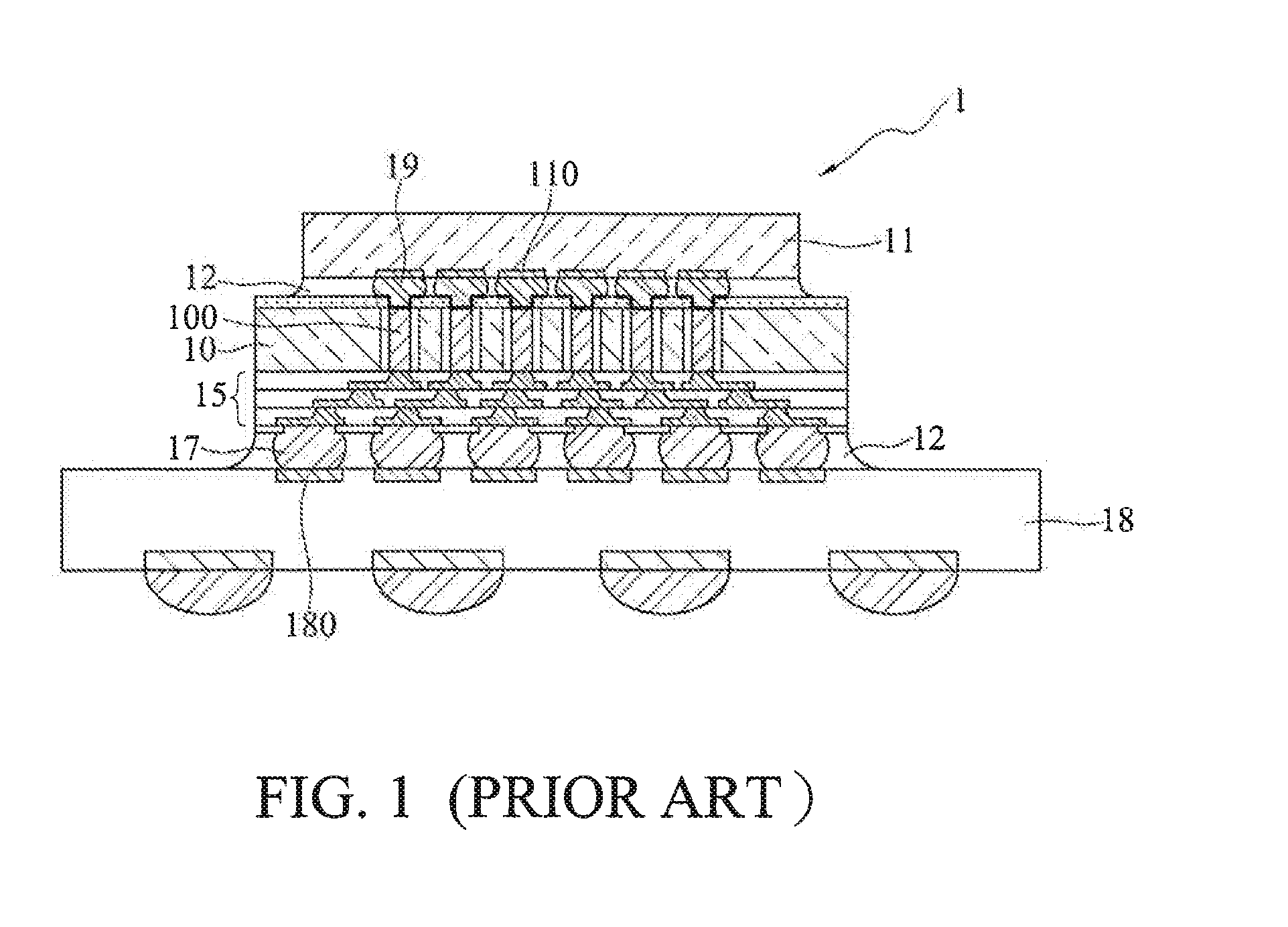
BACKGROUND OF THE INVENTION[0001]1. Field of the Invention[0002]The present invention relates to semiconductor packages and a method of fabricating the same, and, more particularly, to a semiconductor package having wafer level circuits and a method of fabricating the same.[0003]2. Description of the Prior Art[0004]As the technology for developing electronic products is steadily growing, electronic products have now moved to multi-functionality and high functionality. The semiconductor packaging technology has been widely used nowadays to chip scale package (CSP), Direct Chip Attached (DCA), Multi Chip Module (MCM), and 3D-IC stacking technology.[0005]FIG. 1 is a schematic cross-sectional view of a conventional semiconductor package, wherein a through siliconinterposer (TSI) 10 is formed between a substrate 18 and a semiconductor chip 11. The TSI 10 has through-silicon vias (TSV) 100 and a redistribution layer (RDL) 15 formed on the through-silicon via (TSV) 100, allowing the redis...
Claims
Application Information
Patent Timeline
Application Date:The date an application was filed.
Publication Date:The date a patent or application was officially published.
First Publication Date:The earliest publication date of a patent with the same application number.
Issue Date:Publication date of the patent grant document.
PCT Entry Date:The Entry date of PCT National Phase.
Estimated Expiry Date:The statutory expiry date of a patent right according to the Patent Law, and it is the longest term of protection that the patent right can achieve without the termination of the patent right due to other reasons(Term extension factor has been taken into account ).
Invalid Date:Actual expiry date is based on effective date or publication date of legal transaction data of invalid patent.

