Laser Annealing Apparatus and Laser Annealing Method

Active Publication Date: 2015-02-05
SHANGHAI MICRO ELECTRONICS EQUIP (GRP) CO LTD
View PDF4 Cites 12 Cited by
  • Summary
  • Abstract
  • Description
  • Claims
  • Application Information

AI Technical Summary

Benefits of technology

[0024]The laser annealing apparatus and the laser annealing method of the invention can split a single-pulse laser beam into multiple pulsed laser beams according to a desired time delay and an energy ratio and irradiate a target wafer successively with the multiple laser beam

Problems solved by technology

Traditional furnace annealing is incapable of thoroughly eliminating defects in crystals even at a temperature up to 1100° C., while semiconductor laser annealing allows relative thorough removal of such defects.
This will reduce the laser energy utilization efficiency and hence harming the performance of the annealing process.
This problem is commonly associated with conventional single- and double-pulse laser annealing methods.
If elongating the time delay between the two laser pulses,

Method used


Image

  • Laser Annealing Apparatus and Laser Annealing Method
  • Laser Annealing Apparatus and Laser Annealing Method
  • Laser Annealing Apparatus and Laser Annealing Method

Examples


embodiment 2

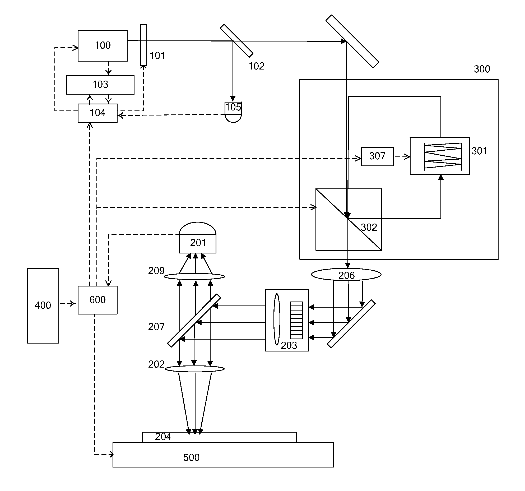
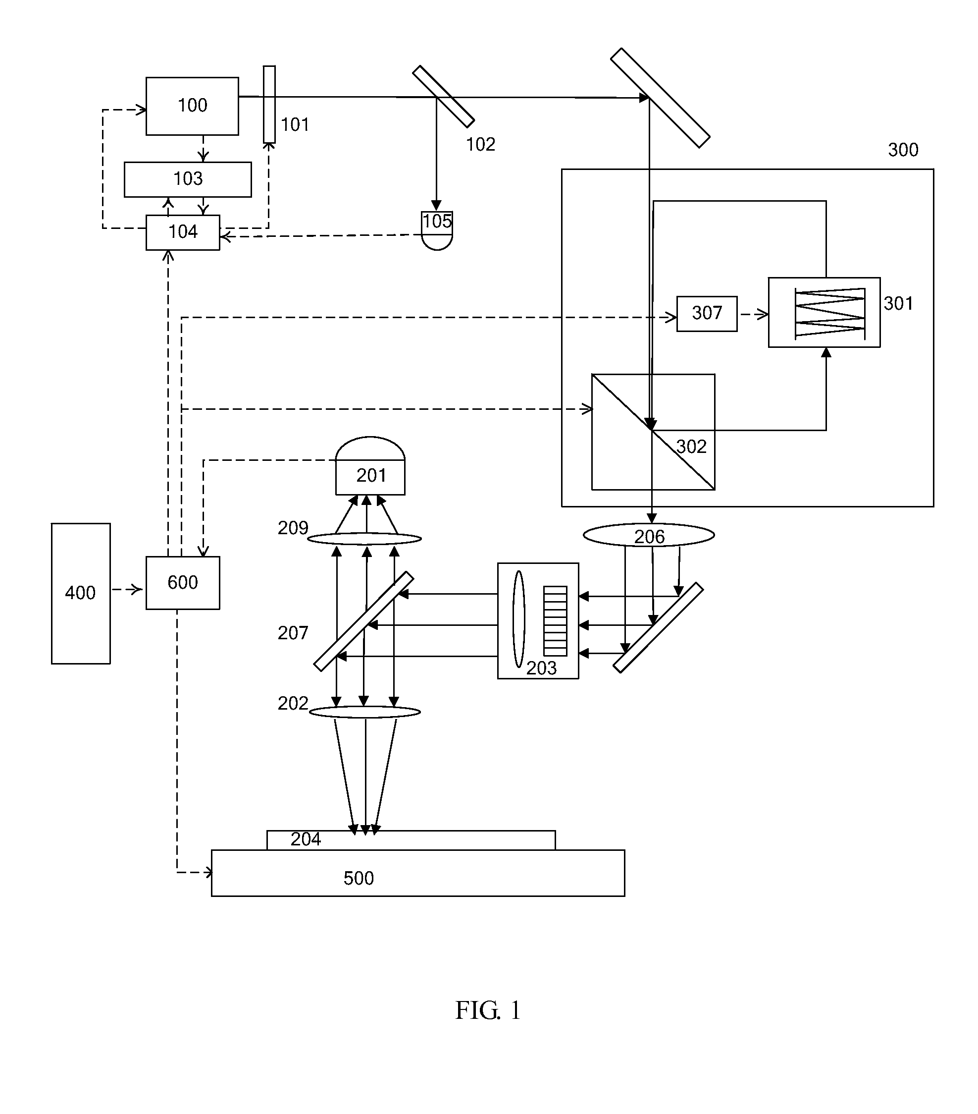
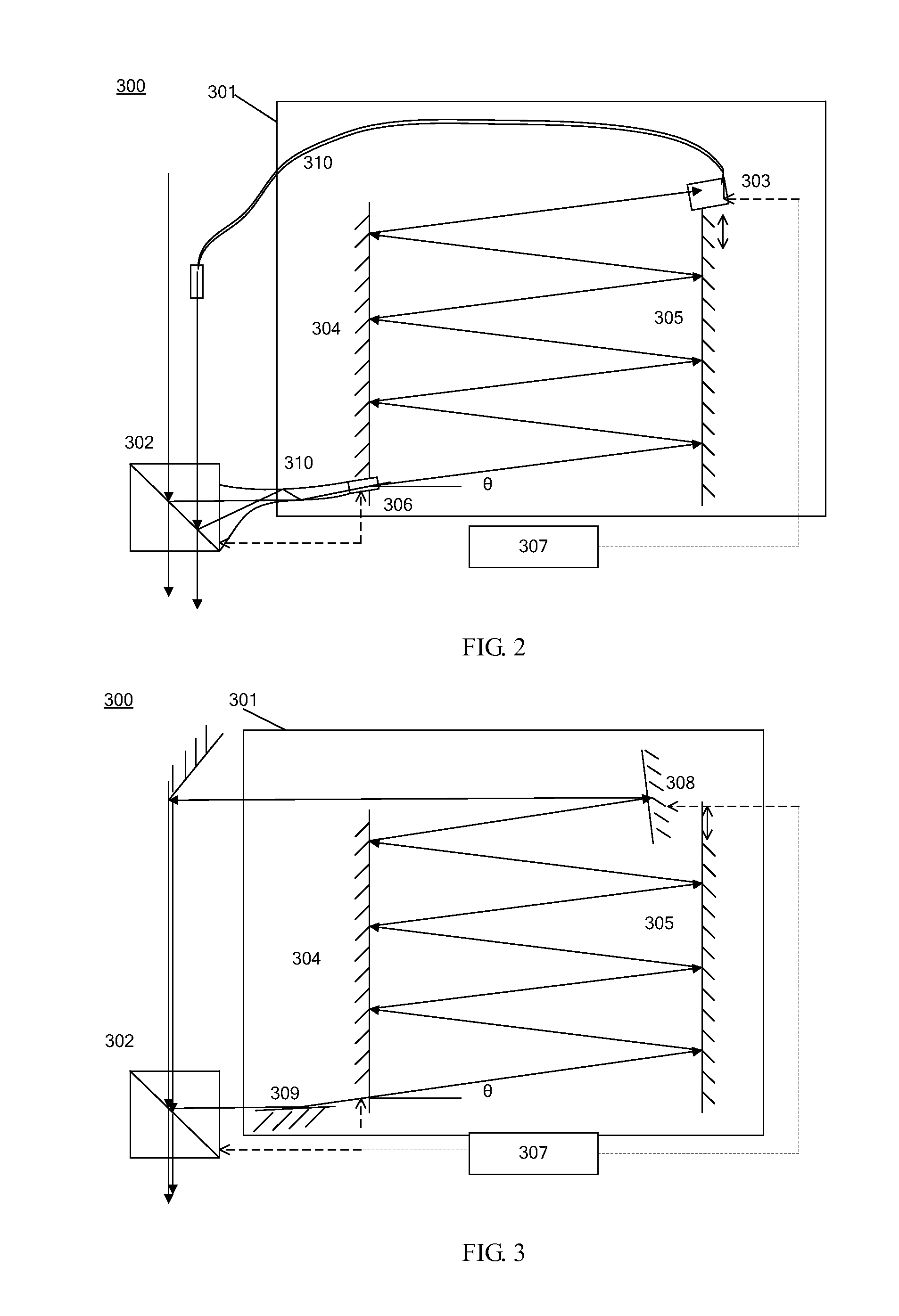
[0066]Referring to FIG. 3 which shows a schematic view of the cyclic delay unit of the laser annealing apparatus in accordance with Embodiment 2 of the present invention, this embodiment differs from Embodiment 1 in: a cyclic delay unit 301 of this embodiment includes two main reflectors 304 and 305, an exit reflector 308 and an entrance reflector 309. Both the exit and entrance reflectors 308 and 309 are adjustable in position. With similarity to the cyclic delay unit of Embodiment 1 described in FIG. 2, this embodiment also has the ability to adjust the total optical path length to allow time delay adjustment. In addition, as the exit and entrance are respectively implemented as the exit and entrance reflectors 308 and 309 in this embodiment, the delayer 301 may accordingly include reflective optical member(s) having the same function of transmitting laser beams in lieu of the optical fibers 310. Similarly, this embodiment can keep the substrate surface temperature around the subs...

embodiment 3

[0067]According to another aspect, the invention also provides a laser annealing method. With reference to FIGS. 1 to 8, the present invention is not limited thereto as the method may employ other annealing apparatuses than those described in the above Embodiments 1 and 2. The method includes:

[0068]providing a stable single-pulse laser beam;

[0069]splitting the single-pulse laser beam into a plurality of pulsed laser beams according to a desired time delay and an energy ratio; and

[0070]irradiating a substrate 204 successively with the plurality of pulsed laser beams to stabilize a surface temperature of the substrate 204 within a predetermined range.

[0071]Preferably, splitting the single-pulse laser beam into the plurality of pulsed laser beams according to the desired time delay and the energy ratio specifically includes:

[0072]a) selecting a first beam splitter according to a preset beam-splitting ratio;

[0073]b) splitting the single-pulse laser beam into two split beams with the fir...


PUM

PropertyMeasurementUnit
Angleaaaaaaaaaa
Timeaaaaaaaaaa
Ratioaaaaaaaaaa

Abstract

A laser annealing apparatus includes: a laser beam generator for providing a stable single-pulse laser; a cyclic delay unit (300) for splitting the single-pulse laser into several pulsed lasers; an optical module for converging one or more of the pulsed lasers on a substrate (204); and a movable stage (500) for providing the substrate (204) with movement in at least one degree of freedom. A laser annealing method includes: providing a stable single-pulse laser; splitting the single-pulse laser into several pulsed lasers according to a delay requirement and an energy ratio; and irradiating a substrate (204) successively with one or more of the pulsed lasers to keep a surface temperature of the wafer around the melting point or around a needed annealing temperature for a sufficiently long time during the annealing process, thus resulting in an improvement in both the laser energy utilization efficiency and effect of the annealing process.

Description

TECHNICAL FIELD[0001]The present invention relates to the field of semiconductor material processing, and in particular, to a laser annealing apparatus and a laser annealing method.BACKGROUND[0002]Annealing is a thermal process to expose a target material to a high temperature for a long time and then cool it down slowly. Traditional furnace annealing is incapable of thoroughly eliminating defects in crystals even at a temperature up to 1100° C., while semiconductor laser annealing allows relative thorough removal of such defects. Laser light wavelengths that can be used in semiconductor laser annealing span a wide spectrum, from the ultraviolet (UV) region to the infrared (IR) region, and there have been developed a variety of semiconductor laser annealing methods, such as the single-pulse laser annealing disclosed in U.S. Pat. No. 6,336,308 (issued on Jan. 8, 2002) and U.S. Pat. No. 7,365,285 (issued on Apr. 29, 2008), high-frequency Q-switch pulsed laser annealing, scanning conti...

Claims


Application Information

Patent Timeline
IPC IPC(8): H01L21/67B23K26/00H01L21/324
CPCH01L21/67115B23K26/0066H01L21/324H01L21/268B23K26/0853H01S3/005B23K26/0006B23K26/0622B23K26/352B23K2101/40B23K2103/56H01S3/00H01S3/0007B23K26/0648B23K26/067
Inventor ZHANG, JUNLI, ZHIDANLI, ZHE
Owner SHANGHAI MICRO ELECTRONICS EQUIP (GRP) CO LTD
Why Eureka
Try Eureka