Patterning of OLED materials

a technology of oled materials and patterns, applied in the direction of organic semiconductor devices, vacuum evaporation coating, thermoelectric devices, etc., can solve the problem that conventional patterning using lithography is not possible with organic materials, and achieve the effect of high resolution and higher resolution

Active Publication Date: 2015-02-12
EMAGIN CORP +1
View PDF0 Cites 36 Cited by
  • Summary
  • Abstract
  • Description
  • Claims
  • Application Information

AI Technical Summary

Benefits of technology

[0008]By using direct patterning of OLED with stencil lithography, high-efficiency, high-resolution OLED microdisplays can be fabricated. In the embodiments disclosed herein, color emitter deposition for OLED uses a shadow mask that can have nm scale features. The shadow masks have precision and accuracy to match the underlying transistor of the microdisplay and create color emitters at higher resolution.

Problems solved by technology

Conventional patterning using lithography is not possible with organics due to the sensitivity of the organics to photoresist and chemistries, which is required for photoresist processing.
Current methods produce color emitter layers with a metal shadow mask, which suffers from resolution issues and may prevent color emitter sub-pixel sizes under 10 μm.

Method used


Image

  • Patterning of OLED materials
  • Patterning of OLED materials
  • Patterning of OLED materials

Examples


example 1

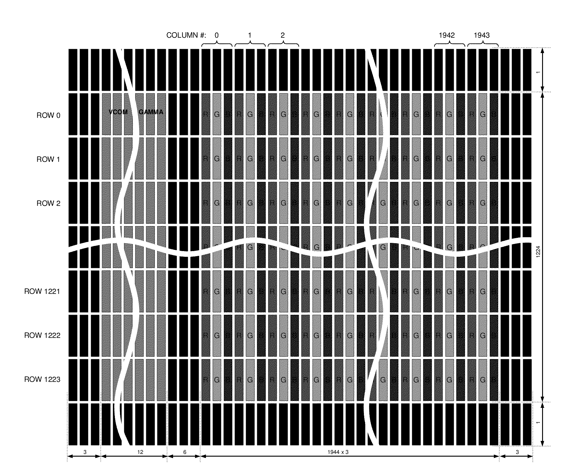
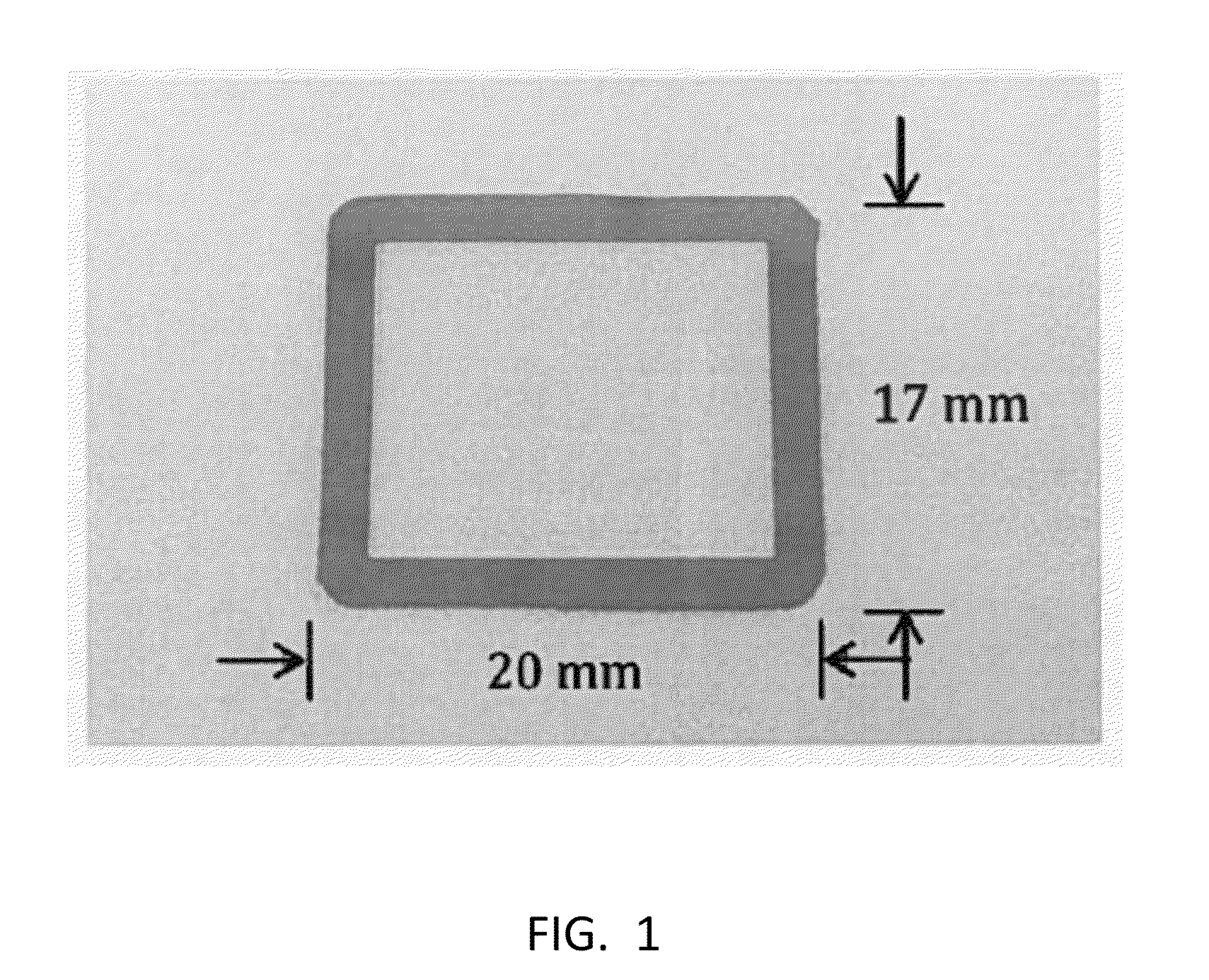
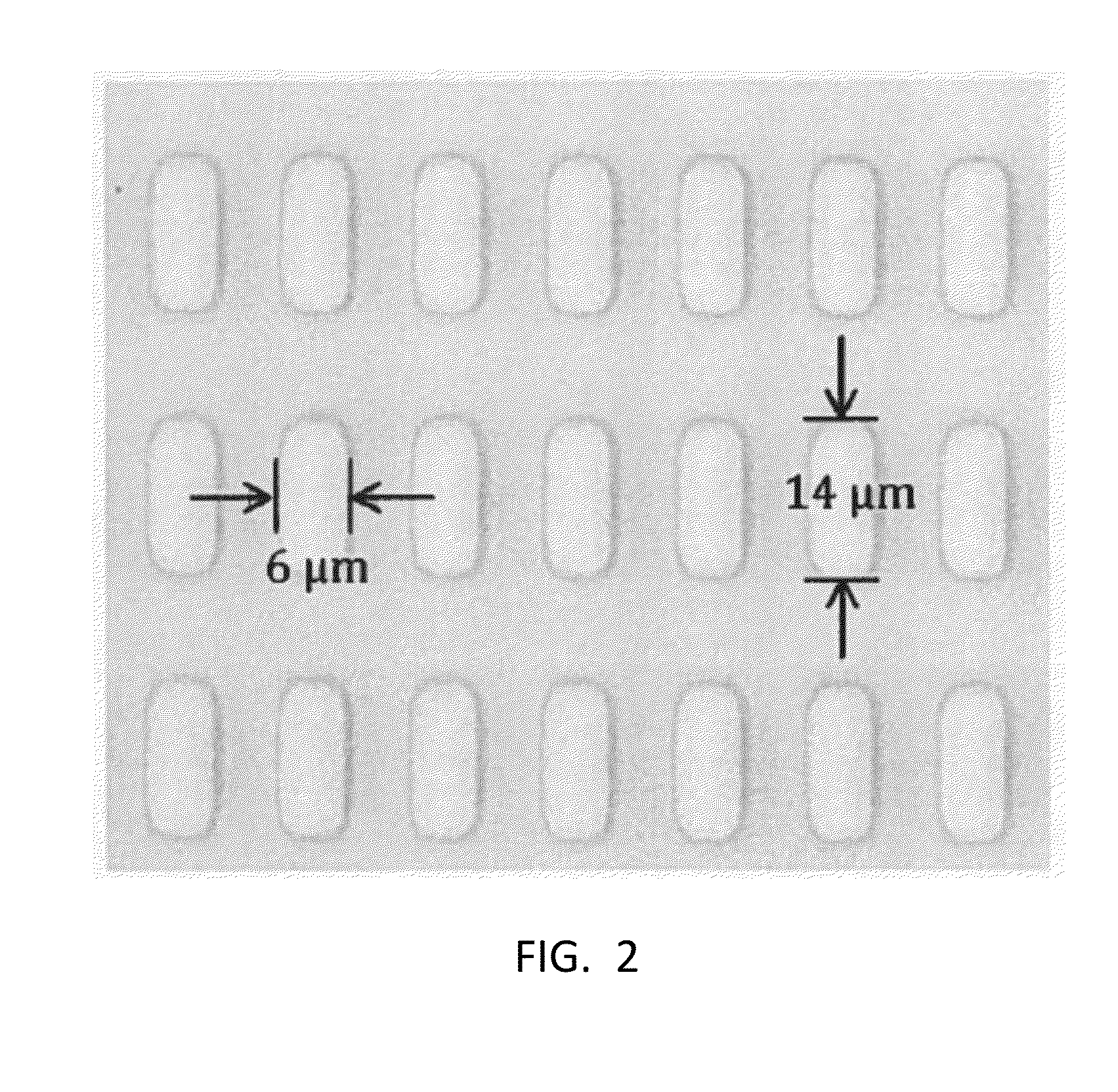
[0115]In this example, fabrication of a shadow mask, deposition of color emitter materials to form a pattern of color emitter structures, and OLED devices having patterned structures of color emitter structures is described.

[0116]Deposition Tool. The tool used for deposition is a rectangular chamber that is 20×19×19 inch and uses an Alcatel 5400 turbo molecular vacuum pump that can reach base pressures of about 5×10⁻⁶ Torr. The depositions performed for this work uses pressures of about 10−5 Torr which gives a mean free path of around 4 m, much greater than the separation of the source to substrate. This allows the depositions to be a function of geometry. In this environment, the organic materials are evaporated or sublimated via resistive heating powered by a Sorensen DCS8-125, where the custom built boats utilizes up to 8 W of power. Deposition rates are determined by quartz crystal monitors that are connected to an “Inficon SQM-242 Thin Film Deposition Controller Card”. An image...


PUM

PropertyMeasurementUnit
sizesaaaaaaaaaa
sizeaaaaaaaaaa
sizeaaaaaaaaaa

Abstract

A method of making a patterned OLED layer or layers. The method uses a shadow mask having, for example, a free-standing silicon nitride membrane to pattern color emitter material with a feature size of less than 10 microns. The methods can be used, for example, in the manufacture of OLED microdisplays.

Description

CROSS-REFERENCE TO RELATED APPLICATIONS[0001]This application claims priority to U.S. provisional patent application No. 61 / 862,685, filed Aug. 6, 2014, the disclosure of which is incorporated herein by reference.FIELD OF THE DISCLOSURE[0002]The present disclosure generally relates to methods for making one or more organic light-emitting diode (OLED) emitter layers. More particularly, the present disclosure relates to direct patterning of one or more OLED layers using shadow masks.BACKGROUND OF THE DISCLOSURE[0003]The OLED diode structure was discovered in 1987, and has been developed into a technology that is used for displays in cellphones, microdisplays and televisions. Microdisplays are small displays that are used under magnification or for projection applications. Some of the applications of microdisplays are camera viewfinders and wearable displays, specifically for professions that require hands free information or for virtual reality applications. GoogHle Glass, currently i...

Claims


Application Information

Patent Timeline
Patent Type & Authority Applications(United States)
IPC IPC(8): H01L51/00H01L51/56H01L27/32
CPCH01L51/0018H01L51/56H01L27/3211C23C14/042H10K59/35H10K71/166H10K50/81H10K50/82H10K71/00H10K71/233H10K50/11H10K50/15H10K50/16H10K85/324H10K85/626H10K85/633H10K2102/00H10K2102/103
Inventor CHAN, CHARLES K.TANG, CHING W.VAZAN, FRIDRICHGHOSH, AMAL
Owner EMAGIN CORP
Why Eureka
Try Eureka