Differential methods and apparatus for metrology of semiconductor targets

a technology of semiconductor targets and differential methods, applied in the direction of semiconductor/solid-state device testing/measurement, photomechanical equipment, instruments, etc., can solve the problems of fewer measurements on a product wafer than on a product wafer, and the difficulty of obtaining plots

Active Publication Date: 2015-02-12
KLA CORP
View PDF26 Cites 108 Cited by
  • Summary
  • Abstract
  • Description
  • Claims
  • Application Information

AI Technical Summary

Problems solved by technology

These plots are generally harder to obtain since measuring these shapes is often a difficult endeavor.
As should be appreciated, using a portion of the device structure may be more difficult, but it tends to be more accurate since it is a portion of the device structure.
Also, fewer measurements are made on a product wafer than on a focus exposure matrix wafer due to time constraints in production.
Using focus solutions determined from many focus exposure matrix measurements can average out measurement errors, stepper errors, and the like.
Although an optimal or best focus can be determined, a lithography tool may actually program a different focus that may be caused by difficulties the tool has in sensing an accurate position of the wafer surface.
That is, it may be difficult for the lithography tool to achieve a particular depth of focus with respect to the actual wafer surface.
A particular optimum depth of focus with respect to a relatively transparent film, such as a photoresist material that is disposed over layers having other grating structures, is especially difficult to achieve.
Consequently, the resulting programmed focus may not be equal to the input best or optimal focus.
This is impossible, or very difficult to model using existing model-based metrology methods.
This output signal cannot be effectively used to determine a process or top structure parameter, such as optimum focus or CD, since such output signal is compromised by the underlying structures.
In general, the difference signals tend to cancel the common unperturbed film signal and leave the contribution due to grating perturbation or defects.

Method used


Image

  • Differential methods and apparatus for metrology of semiconductor targets
  • Differential methods and apparatus for metrology of semiconductor targets
  • Differential methods and apparatus for metrology of semiconductor targets

Examples


Embodiment Construction

[0035]In the following description, numerous specific details are set forth in order to provide a thorough understanding of the present invention. The present invention may be practiced without some or all of these specific details. In other instances, well known process operations have not been described in detail to not unnecessarily obscure the present invention. While the invention will be described in conjunction with the specific embodiments, it will be understood that it is not intended to limit the invention to the embodiments.

INTRODUCTION

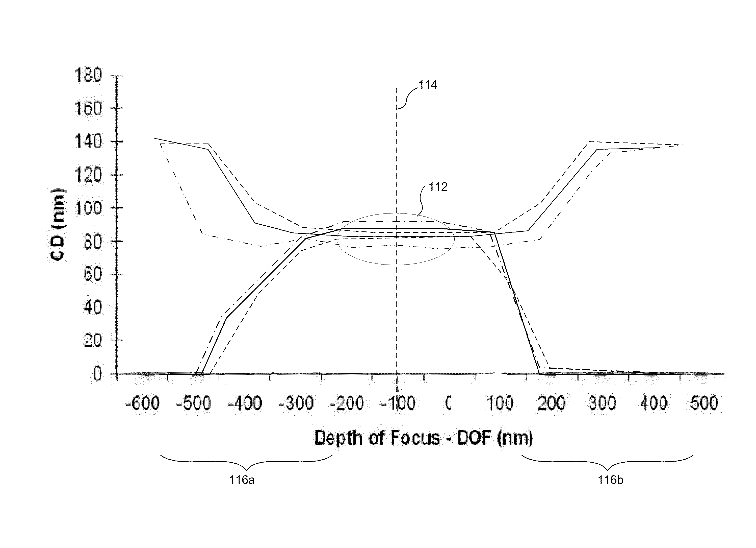
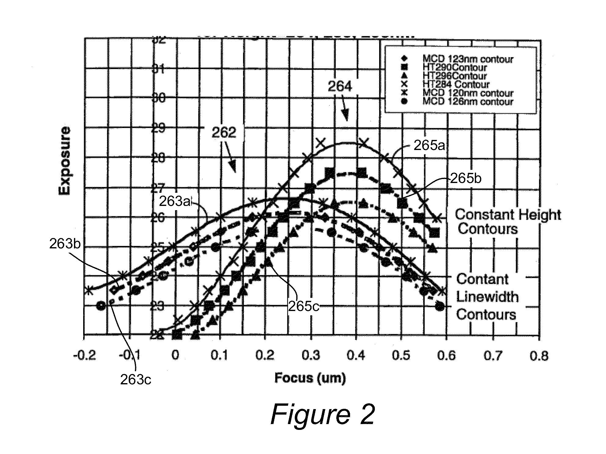
[0036]A focus-exposure matrix obtained from a FEM wafer, by way of example, may be visualized using a Bossung Plot to facilitate determination of a lithography process window. The Bossung Plot generally plots CD vs. focus position for varying levels of exposure, such as the example in FIG. 1. As shown, varying levels of exposure are plotted as contour lines with CD representing the Y axis and focus position representing the X axis of the gr...


PUM

PropertyMeasurementUnit
azimuth angleaaaaaaaaaa
heightaaaaaaaaaa
heightaaaaaaaaaa

Abstract

Disclosed are apparatus and methods for determining process or structure parameters for semiconductor structures. A plurality of optical signals is acquired from one or more targets located in a plurality of fields on a semiconductor wafer. The fields are associated with different process parameters for fabricating the one or more targets, and the acquired optical signals contain information regarding a parameter of interest (POI) for a top structure and information regarding one or more underlayer parameters for one or more underlayers formed below such top structure. A feature extraction model is generated to extract a plurality of feature signals from such acquired optical signals so that the feature signals contain information for the POI and exclude information for the underlayer parameters. A POI value for each top structure of each field is determined based on the feature signals extracted by the feature extraction model.

Description

CROSS-REFERENCE TO RELATED APPLICATIONS[0001]This application claims the benefit of prior application U.S. Provisional Application No. 61 / 864,573, filed 11 Aug. 2013 by Stilian Ivanov Pandev et al., which application is herein incorporated by reference in its entirety for all purposes.TECHNICAL FIELD OF THE INVENTION[0002]The present invention relates generally to methods and systems for determination of process or structure parameters and, more specifically, to determination of process or structure parameters using design of experiment (DOE) or focus exposure matrix (FEM) wafers.BACKGROUND[0003]Photolithography or optical lithography systems used in the manufacture of integrated circuits have been around for some time. Such systems have proven extremely effective in the precise manufacturing and formation of very small details in the product. In most photolithography systems, a circuit image is written on a substrate by transferring a pattern via a light or radiation beam (e.g., UV...

Claims


Application Information

Patent Timeline
Patent Type & Authority Applications(United States)
IPC IPC(8): G01N21/95G01B11/02G01B11/24
CPCG01N21/9501G01N2201/12G01B11/02G01B11/24G01N21/956G03F7/70625G03F7/70641H01L22/12H01L22/30
Inventor PANDEV, STILIAN IVANOVSHCHEGROV, ANDREI V.
Owner KLA CORP
Why Eureka
Try Eureka