Fabrication process and structure to form bumps aligned on TSV on chip backside

a fabrication process and chip backside technology, applied in semiconductor devices, semiconductor/solid-state device details, electrical apparatus, etc., can solve the problems of cu contamination, insufficient protection and isolation of chip backside by passivation, and micro bumps that are needed to form on chip surfaces, etc., to achieve simplified thinning technology of semiconductor layers, increase adhesion area and adhesion strength, and reduce thinning thickness

Inactive Publication Date: 2015-02-19
POWERTECH TECHNOLOGY +1
View PDF9 Cites 16 Cited by
  • Summary
  • Abstract
  • Description
  • Claims
  • Application Information

AI Technical Summary

Benefits of technology

[0004]The main purpose of the present invention is to provide a fabrication process and a structure to fabricate bumps aligned on TSVs on chip backside which can be implemented in via-middle processes to increase the adhesion area and the adhesion strength between bumps and TSV where thinning technology of semiconductor layers can be simplified and the thinning thickness can be reduced. During exposing dielectric liner processes, DRIB can be replaced by conventional etching processes. During exposing TSV processes, CMP can be replaced by selective etching to reduce Cu contamination issues and to reduce the thickness of backside passivation as well as the thickness of the UBM layer to achieve fabricating bumps aligned on TSVs on chip backside with lower cost and higher quality.

Problems solved by technology

Moreover, micro bumps are needed to form on chip surfaces as the interconnection bonding components between vertically stacked chips.
If the extruded height is too small, excessive passivation on chip backside would be removed by CMP where the protection and isolation of chip backside by the passivation may not be sufficient.
Moreover, CMP processes also polish the extruded terminals of TSV leading to Cu contamination issues.
Furthermore, in the conventional structure of fabricating bumps aligned on TSVs on chip backside, the adhesion between bumps and TSV is not enough due to smoother surfaces between bumps and TSV interfaces caused by CMP processes leading to easily-broken bumps.

Method used


Image

  • Fabrication process and structure to form bumps aligned on TSV on chip backside
  • Fabrication process and structure to form bumps aligned on TSV on chip backside
  • Fabrication process and structure to form bumps aligned on TSV on chip backside

Examples


Embodiment Construction

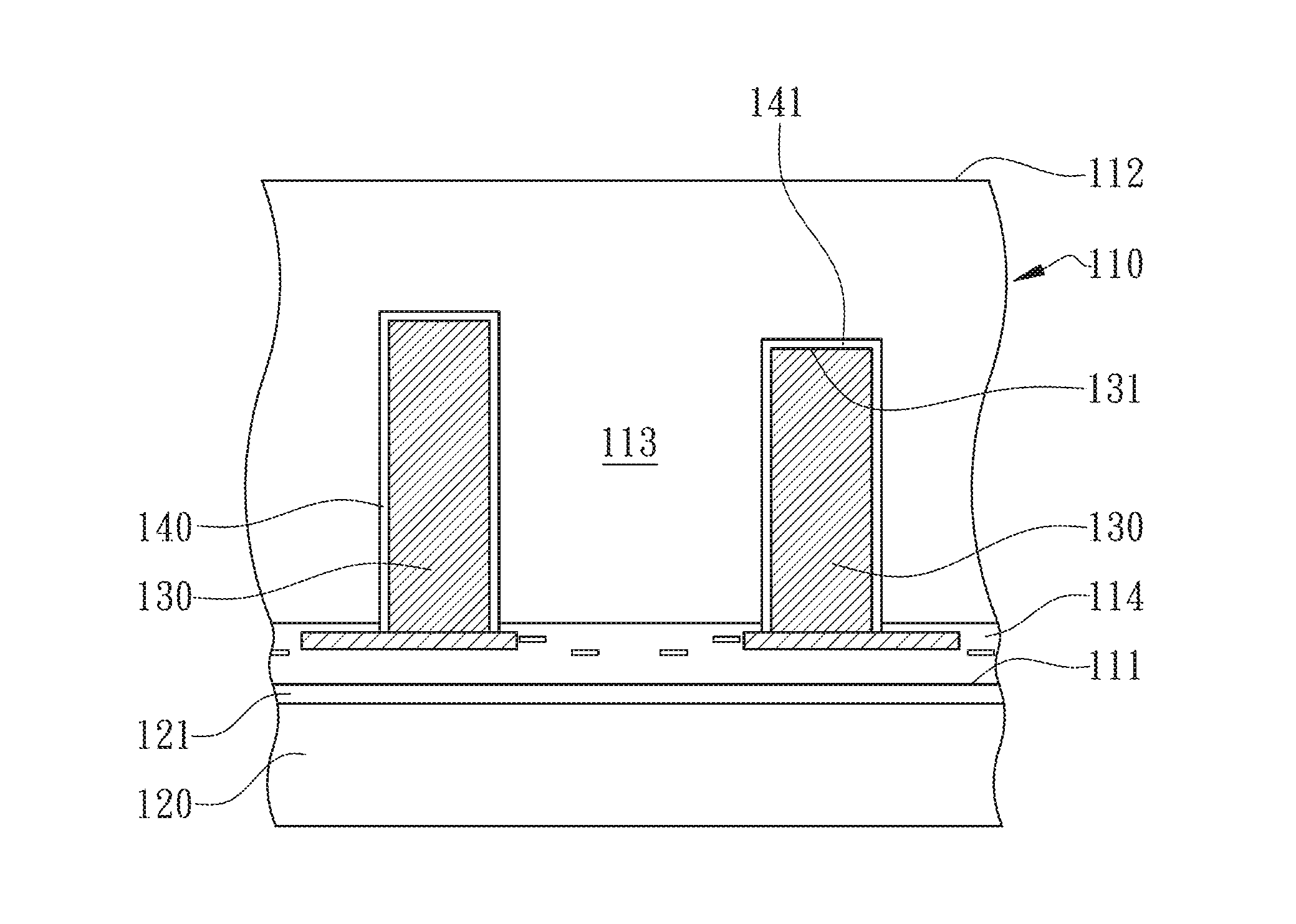
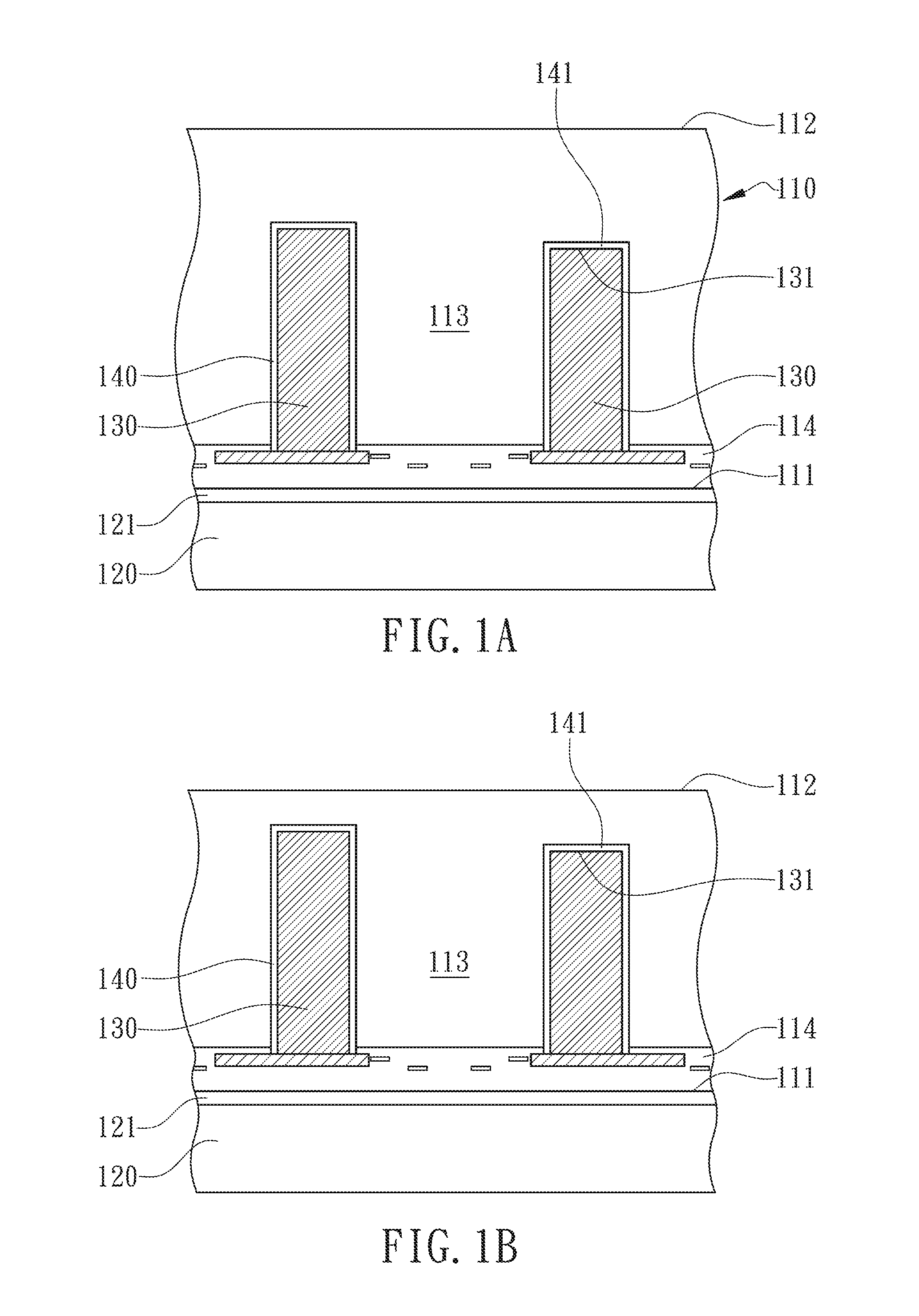
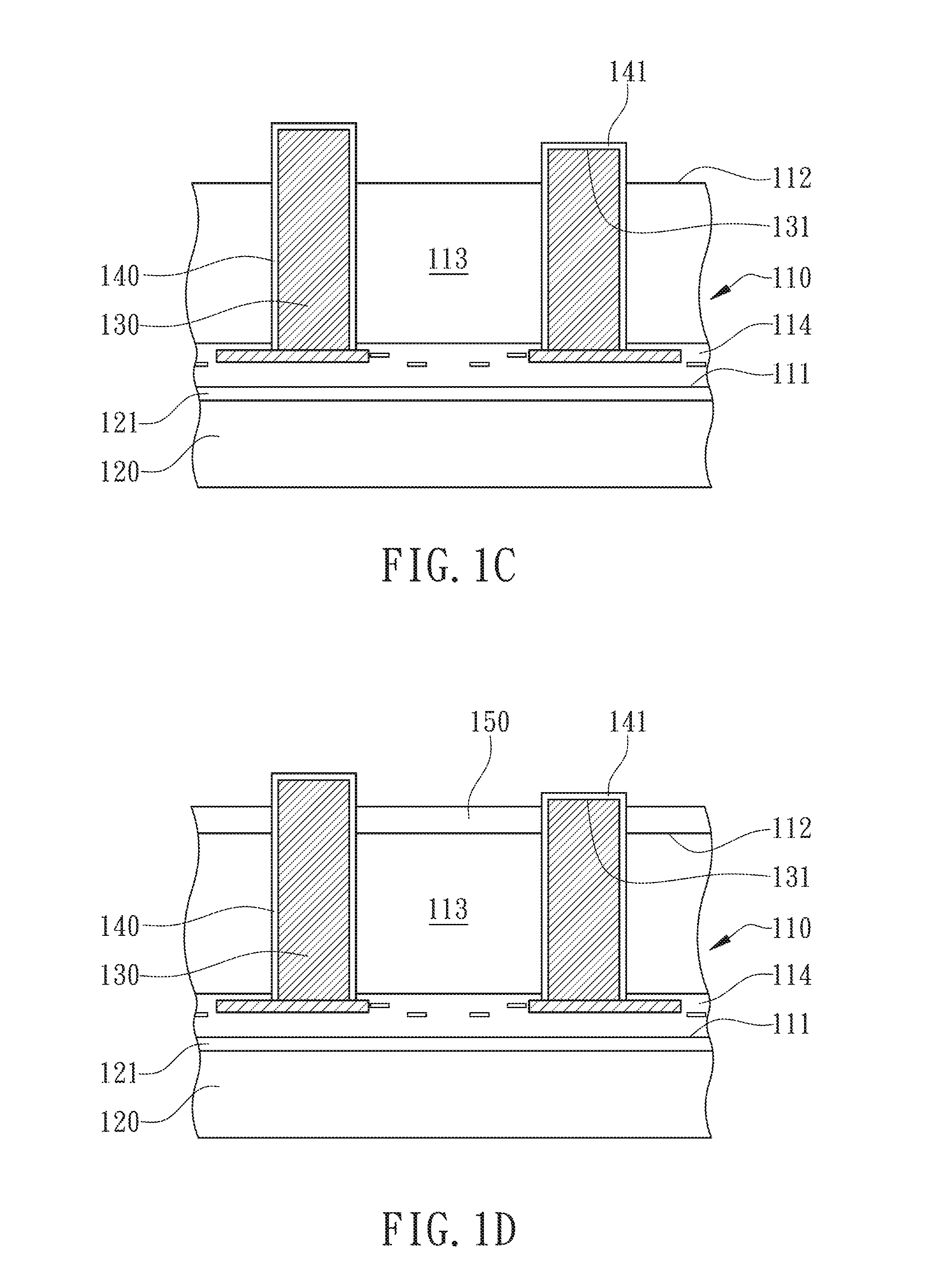
[0007]With reference to the attached drawings, the present invention is described by means of the embodiment(s) below where the attached drawings are simplified for illustration purposes only to illustrate the structures or methods of the present invention by describing the relationships between the components and assembly in the present invention. Therefore, the components shown in the figures are not expressed with the actual numbers, actual shapes, actual dimensions, nor with the actual ratio. Some of the dimensions or dimension ratios have been enlarged or simplified to provide a better illustration. The actual numbers, actual shapes, or actual dimension ratios can be selectively designed and disposed and the detail component layouts may be more complicated.

[0008]According to the preferred embodiment of the present invention, a process to fabricate bumps aligned on TSVs on chip backside are illustrated from FIG. 1A to FIG. 1J for component cross-sectional views. The processes to...


PUM


Abstract

Disclosed is a fabrication process of fabricating bumps aligned on TSVs on chip backside. A plurality of TSV pillars are embedded inside the semiconductor layer of an IC substrate where the sidewalls the bottom of the TSV pillars toward the chip backside are covered by a dielectric liner. Then, the thickness of the semiconductor layer is reduced from the chip backside to make the bottom portion of the dielectric liner to be exposed from the chip backside by including a first selectively etching. Then, a backside passivation is disposed on the chip backside without disposing on the bottoms of the TSV pillars. Then, the bottom portion of the dielectric liner is removed by a second selectively etching. An UBM layer is disposed on the backside passivation. A plurality of bumps are disposed on the UBM layer where the interface between each bump and each TSV pillar is a central protrusion lumped toward the corresponding bump. Accordingly, the interfaces between the bumps and the TSV pillars offer an increased bonding area to increase adhesion anchoring effects for the bumps bonded on the UBM layer through the central protrusions.

Description

FIELD OF THE INVENTION[0001]The present invention relates to a semiconductor device with vertical 3D via interconnection, more specifically to a fabrication process and a structure to form a plurality of bumps aligned on TSV's on chip backside.BACKGROUND OF THE INVENTION[0002]Through Silicon Via (TSV) is implemented in advanced interconnections between semiconductor chips to achieve double-side electrical connection for the fabrication of 3D IC stacking assembly to vertically stack more chips with smaller dimensions. 3D IC stacking technology with TSV is able to continue the development of Moore's Law to fulfill smaller IC chips with higher operation speed and lower power consumption. There are three different process options to form TSV, including via-first, via-middle, and via-last processes. In via first processes, TSVs are formed before IC fabrication. In via middle processes, TSVs are formed after IC fabrication and before back end of line (BEOL) processes. In via last processe...

Claims


Application Information

Patent Timeline
Patent Type & Authority Applications(United States)
IPC IPC(8): H01L23/00
CPCH01L24/10H01L24/11H01L2224/03002H01L21/76898H01L23/481H01L24/03H01L24/05H01L24/06H01L24/13H01L24/14H01L21/6835H01L2221/68327H01L2221/68372H01L2224/0345H01L2224/0361H01L2224/0401H01L2224/05018H01L2224/05025H01L2224/05155H01L2224/05166H01L2224/05181H01L2224/05187H01L2224/05558H01L2224/05575H01L2224/05624H01L2224/05644H01L2224/05647H01L2224/11462H01L2224/1147H01L2224/13025H01L2224/13082H01L2224/131H01L2224/13147H01L2224/1403H01L2224/14051H01L2224/03912H01L2224/11002H01L2224/0601H01L2224/06102H01L2924/00014H01L2924/04941H01L2924/014
Inventor CHIU, CHAO-SHUNCHEN, YEN-CHU
Owner POWERTECH TECHNOLOGY
Why Eureka
Try Eureka