Atomic layer deposition of selected molecular clusters

a molecular cluster and atomic layer technology, applied in the direction of vacuum evaporation coating, semiconductor devices, coatings, etc., can solve the problems of increasing the difficulty of maintaining control of various electrical characteristics of bulk semiconductor devices, and the difficulty of satisfying the requirement to achieve different threshold voltages (vsub>t/sub>) for different devices

Active Publication Date: 2015-02-26
STMICROELECTRONICS SRL
View PDF6 Cites 14 Cited by
  • Summary
  • Abstract
  • Description
  • Claims
  • Application Information

AI Technical Summary

Benefits of technology

[0009]Energy bands of a thin film containing molecular clusters are tuned by controlling the size and the charge of the clusters during thin film deposition. Using atomic layer deposition (ALD), an ionic cluster film is formed in the gate region of a nanometer-scale transistor to adjust the threshold voltage (Vt), and a neutral cluster film is formed in the source and drain regions to adju

Problems solved by technology

As technology nodes for transistors scale below 10 nm, maintaining control of various electrical characteristics in bulk semiconductor devices becomes increasingly more challenging.
For example, circuit designers may choose to place low threshold voltage (LVT) transistors, which are fast but leaky, specifi

Method used


Image

  • Atomic layer deposition of selected molecular clusters
  • Atomic layer deposition of selected molecular clusters
  • Atomic layer deposition of selected molecular clusters

Examples


Embodiment Construction

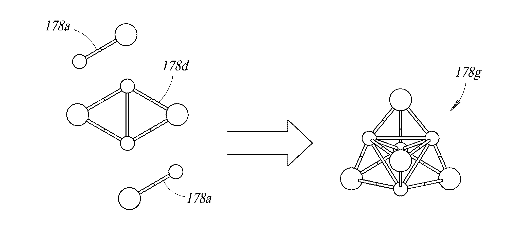
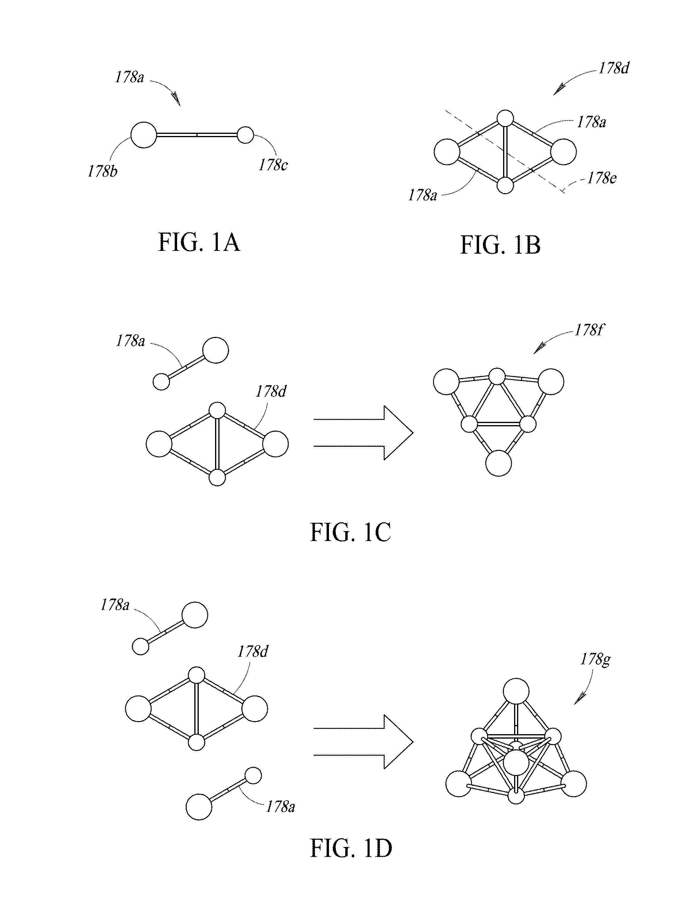
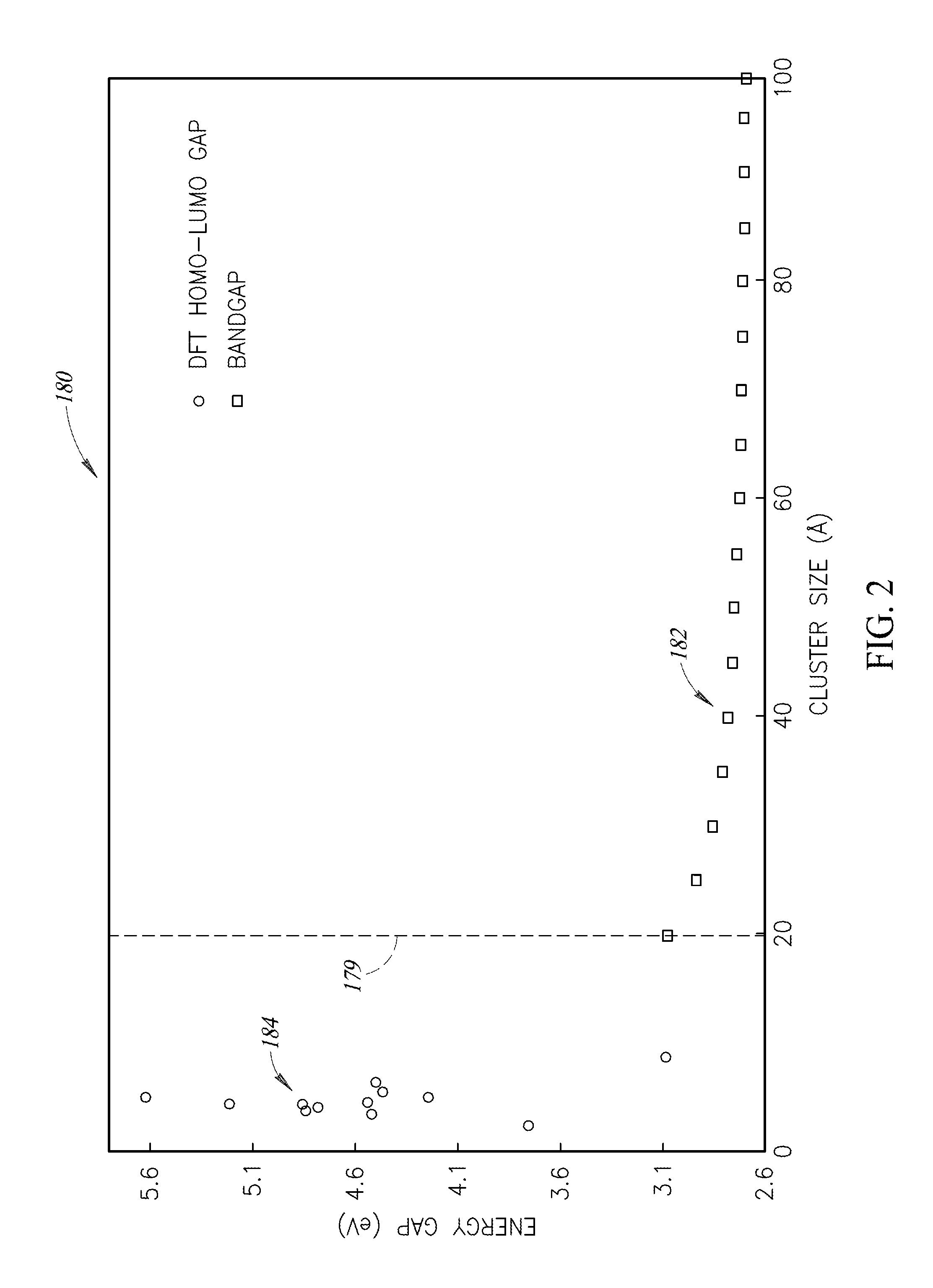
[0027]It will be appreciated that, although specific embodiments of the present disclosure are described herein for purposes of illustration, various modifications may be made without departing from the spirit and scope of the present disclosure. Accordingly, the present disclosure is not limited except as by the appended claims.

[0028]In this description, certain specific details are set forth in order to provide a thorough understanding of various aspects of the disclosed subject matter. However, the disclosed subject matter may be practiced without these specific details. In some instances, well-known structures and methods of semiconductor processing comprising embodiments of the subject matter disclosed herein have not been described in detail to avoid obscuring the descriptions of other aspects of the present disclosure.

[0029]Reference throughout the specification to “one embodiment” or “an embodiment” means that a particular feature, structure, or characteristic described in c...


PUM

PropertyMeasurementUnit
Sizeaaaaaaaaaa
Structureaaaaaaaaaa
Sizeaaaaaaaaaa

Abstract

Energy bands of a thin film containing molecular clusters are tuned by controlling the size and the charge of the clusters during thin film deposition. Using atomic layer deposition, an ionic cluster film is formed in the gate region of a nanometer-scale transistor to adjust the threshold voltage, and a neutral cluster film is formed in the source and drain regions to adjust contact resistance. A work function semiconductor material such as a silver bromide or a lanthanum oxide is deposited so as to include clusters of different sizes such as dimers, trimers, and tetramers, formed from isolated monomers. A type of Atomic Layer Deposition system is used to deposit on semiconductor wafers molecular clusters to form thin film junctions having selected energy gaps. A beam of ions contains different ionic clusters which are then selected for deposition by passing the beam through a filter in which different apertures select clusters based on size and orientation.

Description

RELATED APPLICATION[0001]This patent application claims benefit under 35 U.S.C. §119(e) of U.S. Provisional Patent Application No. 61 / 867,930, filed on Aug. 20, 2013, which is hereby incorporated by reference in its entirety.BACKGROUND[0002]1. Technical Field[0003]The present disclosure relates to the fabrication of nanometer-sized integrated circuit FET (field effect transistor) devices and, in particular, to methods of tuning performance of the FETs by incorporating selected molecular clusters.[0004]2. Description of the Related Art[0005]As technology nodes for transistors scale below 10 nm, maintaining control of various electrical characteristics in bulk semiconductor devices becomes increasingly more challenging. Such electrical characteristics include, for example, transistor threshold voltage and contact resistance. The threshold voltage of a transistor fundamentally governs the transition from an “off” state to an “on” state, and therefore dictates the switching speed and th...

Claims


Application Information

Patent Timeline
IPC IPC(8): H01L29/423H01L29/51H01L29/78
CPCH01L29/42364H01L29/51H01L29/78H01L21/02521H01L21/02631H01L21/28088H01L29/456H01L29/4966H01L29/517H01L29/66545H01L21/823418H01L21/823814H01L21/2855H01L21/76831C23C14/048C23C14/221H01L21/285H01L21/823828H01L21/823807
Inventor ZHANG, JOHN H.
Owner STMICROELECTRONICS SRL
Why Eureka
Try Eureka