Photodetector using surface plasmon resonance and image sensor having the same

a surface plasmon resonance and image sensor technology, applied in the field of photodetectors and image sensors, can solve the problems of inability to sense light having a wavelength greater than 1, and inability to detect light having a wavelength that is inevitably limited, so as to achieve easy control of surface plasmon resonance frequency and easily detect lights

Active Publication Date: 2015-02-26
KOREA INST OF SCI & TECH
View PDF4 Cites 6 Cited by
  • Summary
  • Abstract
  • Description
  • Claims
  • Application Information

AI Technical Summary

Benefits of technology

[0023]Further, it is possible to easily control a surface plasmon resonance frequency of the plasmonic nanostructure by changing a type of metal and a shape factor such as an aspect ratio of a metal. Therefore, unlike a photodetector using a semiconductor...

Problems solved by technology

Accordingly, light having energy that is lower than band gap energy of the semiconductor device is not capable of being sensed.
Therefore, in the case of silicon, it ...

Method used


Image

  • Photodetector using surface plasmon resonance and image sensor having the same
  • Photodetector using surface plasmon resonance and image sensor having the same
  • Photodetector using surface plasmon resonance and image sensor having the same

Examples


Embodiment Construction

[0033]Hereinafter, exemplary embodiments of the present invention will be described in detail with reference to the accompanying drawings so that those skilled in the art may easily practice the present invention. As those skilled in the art would realize, the described embodiments may be modified in various different ways, all without departing from the spirit or scope of the present invention. In addition, the drawings and description are to be regarded as illustrative in nature and not restrictive. Like reference numerals designate like elements throughout the specification. Further, in the present invention, the word “˜on” means positioning on or below a contact surface, but does not essentially mean positioning on the upper side of the contact surface based on a gravity direction.

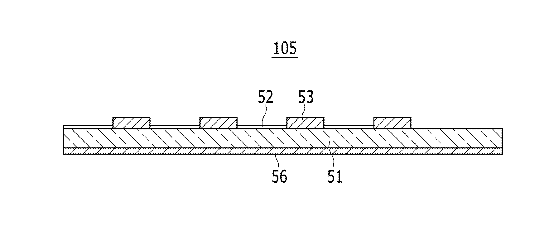
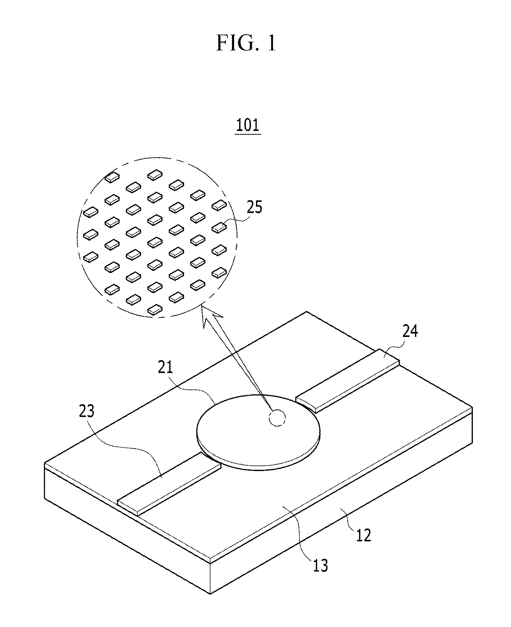
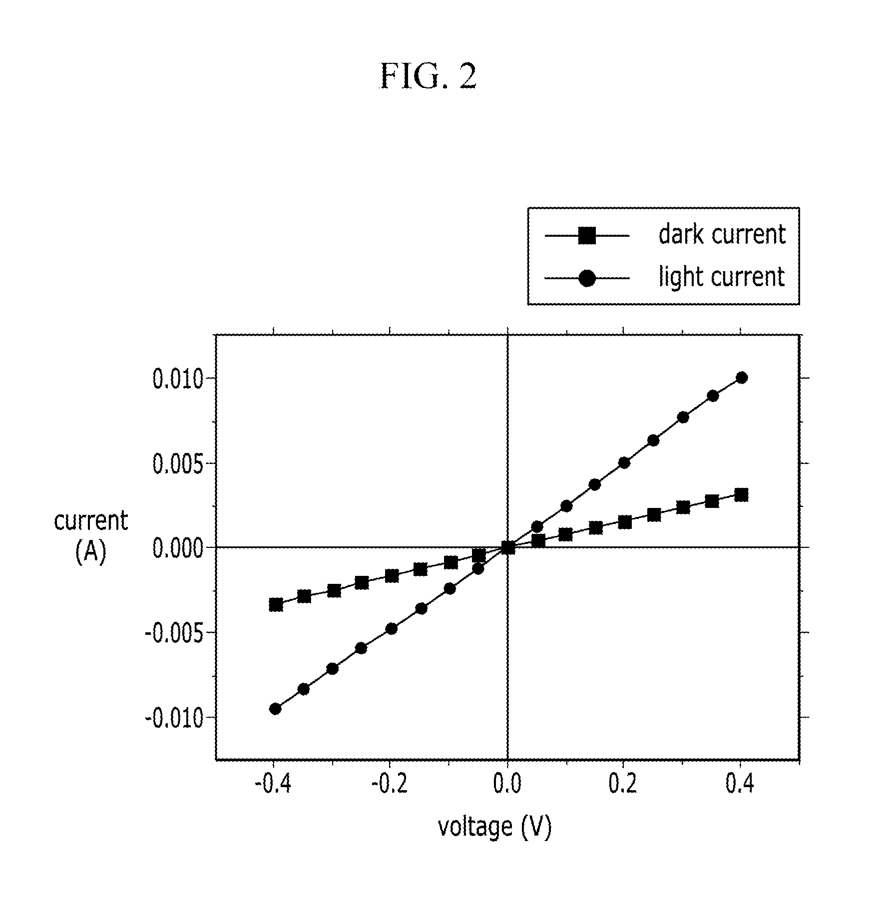
[0034]FIG. 1 is a perspective view showing a photodetector according to a first exemplary embodiment of the present invention, and FIG. 2 is a schematic diagram showing the photodetector according to t...


PUM


Abstract

Disclosed is a photodetector including an electrically conductive substrate, a first electrode formed on the substrate, a second electrode disposed to be spaced apart from the first electrode, a plasmonic nanostructure positioned between the first electrode and the second electrode and having surface plasmon resonance, and a resistance measuring device or an electrical conductivity measuring device connected to the first electrode and the second electrode.

Description

CROSS-REFERENCE TO RELATED APPLICATION[0001]This application claims priority to and the benefit of Korean Patent Application No. 10-2013-0098713 filed in the Korean Intellectual Property Office on Aug. 20, 2013, the entire contents of which are incorporated herein by reference.BACKGROUND[0002](a) Field[0003]The present invention relates to a photodetector and an image sensor. Particularly, the present invention relates to a photodetector using surface plasmon resonance and an image sensor.[0004](b) Description of the Related Art[0005]A known photodetector senses light by using a semiconductor device. A wavelength region of sensed light is determined according to band gap energy of the used semiconductor device. That is, light having energy that is higher than a band gap of the semiconductor device excites electrons of a valence band to a conduction band to change an electrical characteristic of the semiconductor device. Thereby, light is sensed. Accordingly, light having energy that...

Claims


Application Information

Patent Timeline
IPC IPC(8): H01L31/112H01L31/0352H01L27/146
CPCH01L31/1126H01L31/035272H01L27/14638H01L31/0224H01L31/022408H01L31/02327H01L31/09
Inventor LEE, SEUNG YONGSONG, JIN DONGCHO, SO-HYEPARK, JIN OCKPARK, JONG-KU
Owner KOREA INST OF SCI & TECH
Why Eureka
Try Eureka