

Polycrystalline silicon ingot, preparation method thereof, and polycrystalline silicon wafer
a polycrystalline silicon and ingot technology, applied in the field of semiconductor manufacturing, can solve the problems of low photoelectric conversion efficiency of solar cells produced by such polycrystalline silicon ingots, low quality of polycrystalline silicon ingots obtained by this method, and dislocations caused by dislocations, etc., to achieve good initial nucleation, reduce dislocations, and high quality
- Summary
- Abstract
- Description
- Claims
- Application Information
AI Technical Summary
Benefits of technology
Problems solved by technology
Method used
Image

Examples
example 1
[0111]A method for preparing polycrystalline silicon ingot.
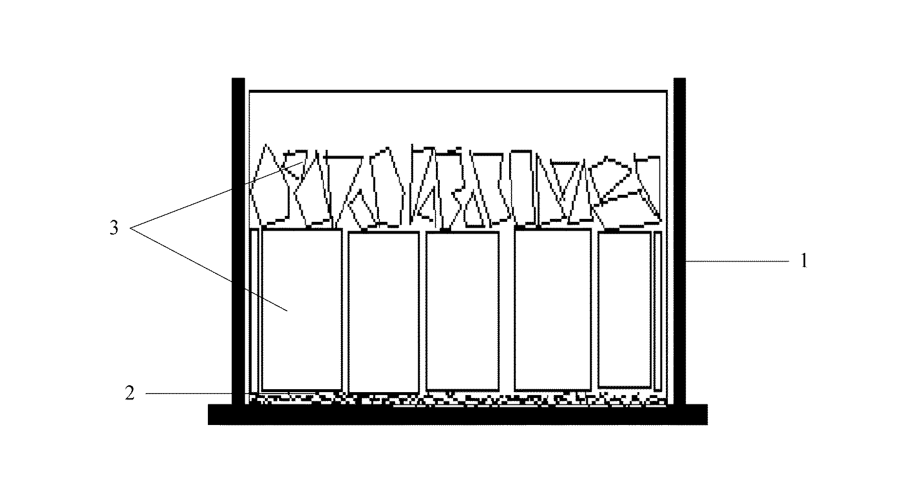
[0112]A layer of silicon nitride was provided on inner wall of a quartz crucible by spray coating, followed by laying a layer of crushed polycrystalline silicon having a size of 1-5 cm at the bottom of the crucible. The layer of crushed polycrystalline silicon was 1 cm. Then various chunk silicon was fed onto crushed polycrystalline silicon until the crucible was full. FIG. 1 is a schematic view of one embodiment, showing the crucible after feeding. 1 is crucible, 2 is crushed polycrystalline silicon and 3 is silicon.
[0113]The crucible filled with silicon was then placed into a casting furnace. Starting a casting ingot program and vacuuming. And the temperature was elevated to the melting point of silicon by heating so as to melt the silicon slowly. During the melting process, solid-liquid interface formed by molten silicon and unmelted silicon was detected by using quartz rob. In preliminary stage of the melting process, th...
example 2
[0120]A method for preparing polycrystalline silicon ingot.
[0121]A layer of silicon nitride was provided on inner wall of a quartz crucible by spray coating. And then a layer of chunk polycrystalline silicon was laid at the bottom of the crucible, followed by laying a layer of crushed polycrystalline material having a size of 1-5 cm. Thickness of the layer of chunk polycrystalline silicon was 1 cm. Thickness of the layer of crushed polycrystalline material was 2 cm. After that, various chunk silicon was fed onto crushed polycrystalline material until the crucible was full.
[0122]The crucible filled with silicon was then placed into a casting furnace. Starting a casting ingot program and vacuuming. And the temperature was elevated to the melting point of silicon by heating so as to melt the silicon slowly. During the melting process, solid-liquid interface formed by molten silicon and unmelted silicon was detected by using quartz rob. In preliminary stage of the melting process, the p...
example 3
[0128]A method for preparing polycrystalline silicon ingot.
[0129]A layer of silicon nitride was provided on inner wall of a quartz crucible by spray coating. And then a layer of graphite plate of high strength, high density and high purity was laid at the bottom of the crucible, followed by laying a layer of crushed polycrystalline material having a size of 1-5 cm. Thickness of the layer of graphite plate was 1 cm. Thickness of the layer of crushed polycrystalline material was 0.5 cm. After that, various chunk silicon was fed onto crushed polycrystalline material until the crucible was full.
[0130]The crucible filled with silicon was then placed into a casting furnace. Starting a casting ingot program and vacuuming. And the temperature was elevated to the melting point of silicon by heating so as to melt the silicon slowly. During the melting process, solid-liquid interface formed by molten silicon and unmelted silicon was detected by using quartz rob. In preliminary stage of the mel...
PUM
| Property | Measurement | Unit |
|---|---|---|
| height | aaaaa | aaaaa |
| height | aaaaa | aaaaa |
| height | aaaaa | aaaaa |
Abstract
Description
Claims
Application Information