Supercharge Your Innovation With Domain-Expert AI Agents!

Polycrystalline silicon ingot and preparation method thereof as well as polycrystalline silicon wafer

A technology of polycrystalline silicon ingots and silicon materials, which is applied to the growth of polycrystalline materials, chemical instruments and methods, and crystal growth, etc., can solve the problems of low photoelectric conversion efficiency of solar cells, low quality of polycrystalline silicon ingots, and uneven crystal grains. Improved conversion efficiency, reduced dislocation propagation, and simple operation

Active Publication Date: 2012-11-14
JIANGXI SAI WEI LDK SOLAR HI TECH CO LTD
View PDF5 Cites 24 Cited by
  • Summary
  • Abstract
  • Description
  • Claims
  • Application Information

AI Technical Summary

Problems solved by technology

However, since the initial nucleation is not controlled, dislocations are easily generated during the nucleation process, resulting in disordered crystal orientation and uneven grains, so the quality of polycrystalline silicon ingots prepared by this method is low
The photoelectric conversion efficiency of solar cells made from this polycrystalline silicon ingot is low

Method used


Image

  • Polycrystalline silicon ingot and preparation method thereof as well as polycrystalline silicon wafer
  • Polycrystalline silicon ingot and preparation method thereof as well as polycrystalline silicon wafer
  • Polycrystalline silicon ingot and preparation method thereof as well as polycrystalline silicon wafer

Examples


Embodiment 1

[0046] A method for preparing a polycrystalline silicon ingot, comprising:

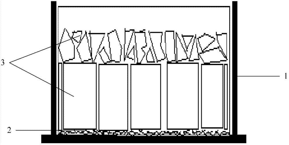
[0047] Take a quartz crucible, spray a layer of silicon nitride coating on the inner wall of the crucible, and lay a layer of polysilicon scraps with a size of 1-5 cm and a thickness of 1 cm on the bottom of the crucible. After laying the bedding, fill various block silicon materials on the polysilicon scraps until all of them are filled. figure 1 It is a schematic diagram of this embodiment after charging, wherein 1 is a crucible, 2 is polysilicon scrap, and 3 is silicon material.

[0048] Put the above-mentioned crucible with silicon material into the ingot casting furnace, start the ingot casting process, vacuumize, and then heat to the melting point of silicon to slowly melt the silicon material. In the melting stage, use a quartz rod to detect the position of the solid-liquid interface formed by the silicon melt and unmelted silicon material. In the early stage of the melting stage, the detectio...

Embodiment 2

[0056] A method for preparing a polycrystalline silicon ingot, comprising:

[0057] Take a quartz crucible, and spray a layer of silicon nitride coating on the inner wall of the crucible. First lay a layer of polysilicon block with a thickness of 1 cm on the bottom of the crucible, and then lay a layer of polycrystalline scrap with a size of 1 to 5 cm and a thickness of 2 cm on it. After laying the bedding, fill various block silicon materials on the polycrystalline crumbs until all of them are filled.

[0058] Put the above-mentioned crucible with silicon material into the ingot casting furnace, start the ingot casting process, vacuumize, and then heat to the melting point of silicon to slowly melt the silicon material. In the melting stage, use a quartz rod to detect the position of the solid-liquid interface formed by the silicon melt and unmelted silicon material. In the early stage of the melting stage, the detection is carried out every 1h, and in the late stage of the ...

Embodiment 3

[0065] A method for preparing a polycrystalline silicon ingot, comprising:

[0066] Take a quartz crucible, and spray a layer of silicon nitride coating on the inner wall of the crucible. First lay a layer of graphite plate with a thickness of 1cm on the bottom of the crucible. The graphite material is three-high graphite, and then lay a layer of polycrystalline scrap with a size of 1-5cm and a thickness of 0.5cm on it. After laying the bedding, fill various block silicon materials on the polycrystalline crumbs until all of them are filled.

[0067] Put the above-mentioned crucible with silicon material into the ingot casting furnace, start the ingot casting process, vacuumize, and then heat to the melting point of silicon to slowly melt the silicon material. In the melting stage, use a quartz rod to detect the position of the solid-liquid interface formed by the silicon melt and unmelted silicon material. In the early stage of the melting stage, the detection is carried out ...


PUM

PropertyMeasurementUnit
thicknessaaaaaaaaaa
thicknessaaaaaaaaaa
sizeaaaaaaaaaa

Abstract

The invention discloses a preparation method of a polycrystalline silicon ingot, comprising the following steps of: filling a silicon mixture in a crucible from bottom to top after coating a silicon nitride layer on the inner wall of the crucible; heating the crucible so that the silicon mixture in the crucible is melted to form a silicon melt, and when a solid-liquid interface formed by the silicon melt and an unmelted silicon mixture approaches to the bottom surface of the crucible, regulating a thermal field to form a supercooled state, so that the silicon melt carries out crystal growth on the basis of the silicon mixture which is not completely melted; and after crystallization of all the silicon melt, annealing and cooling to obtain the polycrystalline silicon ingot. With the adoption of the preparation method, the polycrystalline silicon ingot can have good initial nucleation, and dislocation propagation of the polycrystalline silicon ingot in the growth process is lowered. The invention also discloses the polycrystalline silicon ingot acquired through the preparation method and a polycrystalline silicon wafer prepared with the polycrystalline silicon ingot as a raw material.

Description

technical field [0001] The invention relates to the field of semiconductor manufacturing, in particular to a polycrystalline silicon ingot, a preparation method thereof and a polycrystalline silicon chip. Background technique [0002] In recent years, solar energy, as an emerging renewable green energy, has become a hotspot of development and research. With the rapid development of the solar cell industry, polysilicon, which is low in cost and suitable for large-scale production, has become one of the most important photovoltaic materials in the industry, and has gradually replaced the traditional Czochralski monocrystalline silicon in the solar cell material market. [0003] At present, the preparation method of polycrystalline silicon ingot mainly adopts the directional solidification system method (DSS for short) furnace crystal growth technology provided by GT Solar, and this method usually includes steps such as heating, melting, solidification growth, annealing and coo...

Claims


Application Information

Patent Timeline
Patent Type & Authority Applications(China)
IPC IPC(8): C30B11/00C30B28/06C30B29/06
Inventor 何亮胡动力张涛雷琦万跃鹏
Owner JIANGXI SAI WEI LDK SOLAR HI TECH CO LTD
Features
  • R&D
  • Intellectual Property
  • Life Sciences
  • Materials
  • Tech Scout
  • Unparalleled Data Quality
  • Higher Quality Content
  • 60% Fewer Hallucinations
Learn More