Supercharge Your Innovation With Domain-Expert AI Agents!

A kind of polycrystalline silicon ingot and its preparation method and polycrystalline silicon chip

A technology for polycrystalline silicon ingots and silicon materials, which is applied to the growth of polycrystalline materials, chemical instruments and methods, and crystal growth, etc., can solve the problems of uneven crystal grains, low quality of polycrystalline silicon ingots, and disordered crystal orientations, so as to improve the photoelectric conversion efficiency. , The effect of reducing dislocation propagation and low dislocation density

Active Publication Date: 2015-09-16
JIANGXI SAI WEI LDK SOLAR HI TECH CO LTD
View PDF3 Cites 0 Cited by
  • Summary
  • Abstract
  • Description
  • Claims
  • Application Information

AI Technical Summary

Problems solved by technology

However, since the initial nucleation is not controlled, dislocations are easily generated during the nucleation process, resulting in disordered crystal orientation and uneven grains, so the quality of polycrystalline silicon ingots prepared by this method is low
The photoelectric conversion efficiency of solar cells made from this polycrystalline silicon ingot is low

Method used


Image

  • A kind of polycrystalline silicon ingot and its preparation method and polycrystalline silicon chip
  • A kind of polycrystalline silicon ingot and its preparation method and polycrystalline silicon chip
  • A kind of polycrystalline silicon ingot and its preparation method and polycrystalline silicon chip

Examples


Embodiment 1

[0036] A method for preparing polycrystalline silicon ingots, including:

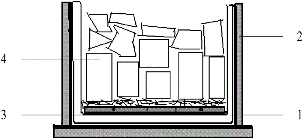
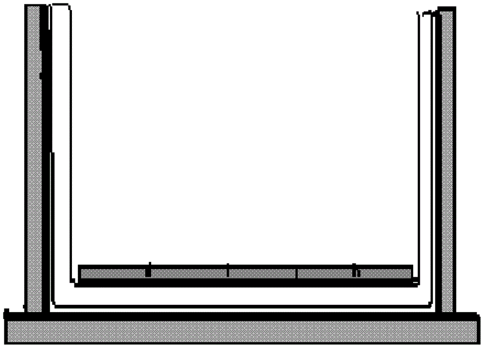
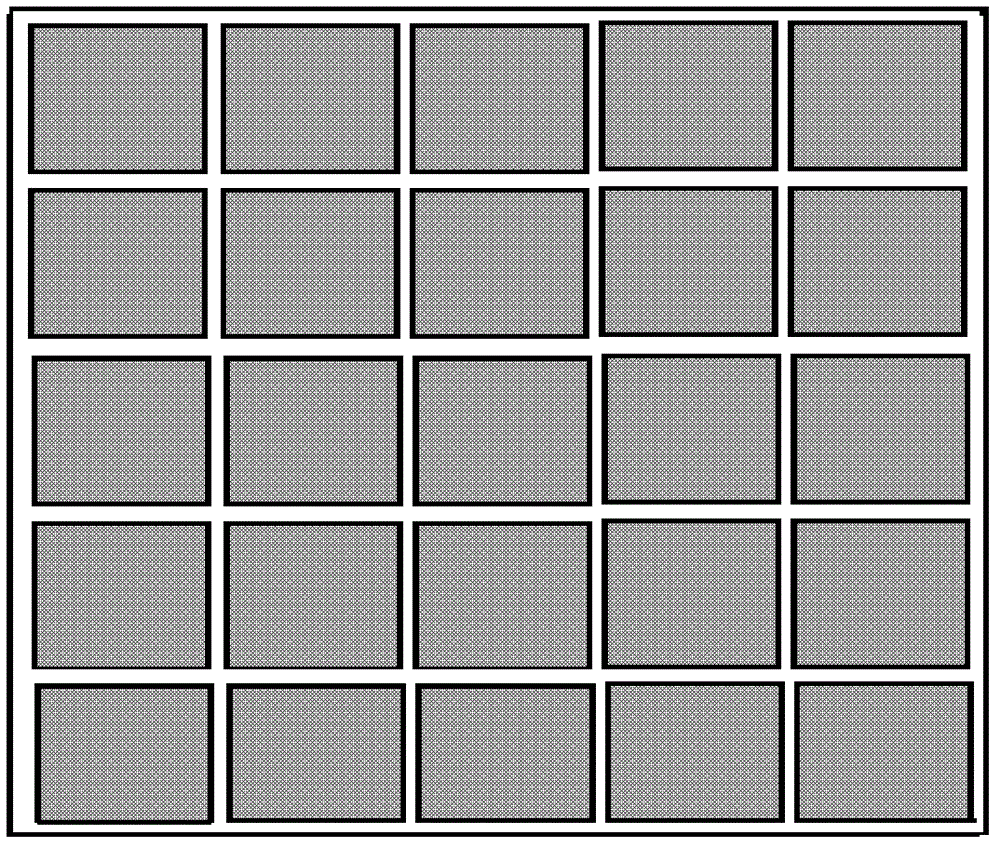
[0037] Using a quartz crucible, spray a layer of silicon nitride coating on the inner wall of the crucible. On the bottom of the crucible, 25 square silicon nitride porous materials with a size of 155mm×155mm were laid. After laying the foundation, fill the silicon nitride porous material with silicon material until it is completely filled. Figure 1~3 This is a schematic diagram of charging in this embodiment, figure 1 1 is a crucible, 2 is a graphite guard plate, 3 is a porous silicon nitride material, and 4 is a silicon material.

[0038] Put the above crucible containing silicon material into the ingot casting furnace, start the ingot casting program, evacuate, and then heat to the melting point temperature of silicon, and let the silicon material slowly melt to form a silicon melt. After the silicon material is completely melted, the heat insulation cage is slowly opened and the temperature is lowered...

Embodiment 2

[0044] A method for preparing polycrystalline silicon ingots, including:

[0045] Using a quartz crucible, spray a layer of silicon nitride coating on the inner wall of the crucible. At the bottom of the crucible, 25 square silicon carbide porous materials with a size of 155×155 mm were laid. After the laying is completed, the silicon carbide porous material is filled with silicon material until it is completely filled.

[0046] Put the above crucible containing silicon material into the ingot casting furnace, start the ingot casting program, evacuate, and then heat to the melting point temperature of silicon, and let the silicon material slowly melt to form a silicon melt. After the silicon material is completely melted, the heat insulation cage is slowly opened and the temperature is lowered, so that the temperature of the silicon melt is reduced to form a supercooled state, and nucleation and crystallization.

[0047] Wait until the directional solidification of the silicon ingo...

Embodiment 3

[0052] A method for preparing polycrystalline silicon ingots, including:

[0053] Using a quartz crucible, spray a layer of silicon nitride coating on the inner wall of the crucible. At the bottom of the crucible, 25 pieces of square quartz porous material with a size of 155×155mm were laid. After laying the foundation, fill the silica material on the porous quartz material until it is completely filled.

[0054] Put the above crucible containing silicon material into the ingot casting furnace, start the ingot casting program, evacuate, and then heat to the melting point temperature of silicon, and let the silicon material slowly melt to form a silicon melt. After the silicon material is completely melted, the heat insulation cage is slowly opened and the temperature is lowered, so that the temperature of the silicon melt is reduced to form a supercooled state, and nucleation and crystallization.

[0055] Wait until the directional solidification of the silicon ingot is complete. ...


PUM

PropertyMeasurementUnit
sizeaaaaaaaaaa
thicknessaaaaaaaaaa
pore sizeaaaaaaaaaa

Abstract

The invention discloses a preparation method of a polycrystalline silicon ingot. The preparation method comprises the steps that after a layer of silicon nitride is coated on the inner wall of a crucible, a layer of porous materials are paved on the bottom of the crucible, and then, silicon materials are filled on the porous materials; the crucible filled with silicon materials is heated, the silicon materials are molten to form silicon melts, then, a heat field is regulated, and the silicon melts start to form core crystallization; and when silicon melt interfaces move in a direction away from the bottom of the crucible, and the directional crystallization solidification is completed, the polycrystalline silicon ingot is obtained through annealing cooling. When the preparation method is adopted, the polycrystalline silicon ingot can obtain good initial nucleation, and the dislocation propagation of the polycrystalline silicon ingot in the growth process is reduced. The invention also simultaneously discloses the polycrystalline silicon ingot obtained by the preparation method, and a polycrystalline silicon slice prepared by using the polycrystalline silicon ingot as raw materials.

Description

Technical field [0001] The invention relates to the field of semiconductor manufacturing, in particular to a polycrystalline silicon ingot, a preparation method thereof, and a polycrystalline silicon wafer. Background technique [0002] In recent years, solar energy as an emerging renewable green energy has become a hot spot for development and research. With the rapid development of the solar cell industry, polycrystalline silicon, which is low-cost and suitable for large-scale production, has become one of the most important photovoltaic materials in the industry, and has gradually replaced the traditional Czochralski monocrystalline silicon in the solar cell material market. [0003] At present, the preparation method of polycrystalline silicon ingots mainly adopts the directional solidification system method (DSS) furnace crystal growth technology provided by GT Solar, which usually includes heating, melting, solidification and crystal growth, annealing and cooling. In the pro...

Claims


Application Information

Patent Timeline
Patent Type & Authority Patents(China)
IPC IPC(8): C30B11/00C30B28/06C30B29/06
Inventor 何亮胡动力张涛雷琦
Owner JIANGXI SAI WEI LDK SOLAR HI TECH CO LTD
Features
  • R&D
  • Intellectual Property
  • Life Sciences
  • Materials
  • Tech Scout
  • Unparalleled Data Quality
  • Higher Quality Content
  • 60% Fewer Hallucinations
Learn More