A kind of polycrystalline silicon ingot and its preparation method and polycrystalline silicon chip
A technology of polycrystalline silicon ingots and silicon materials, which is applied to the growth of polycrystalline materials, chemical instruments and methods, and crystal growth, etc., can solve the problems of low photoelectric conversion efficiency of solar cells, low quality of polycrystalline silicon ingots, and uneven crystal grains. Improved conversion efficiency, reduced dislocation propagation, and simple operation
- Summary
- Abstract
- Description
- Claims
- Application Information
AI Technical Summary
Problems solved by technology
Method used
Image
Examples
Embodiment 1
[0046] A method for preparing a polycrystalline silicon ingot, comprising:
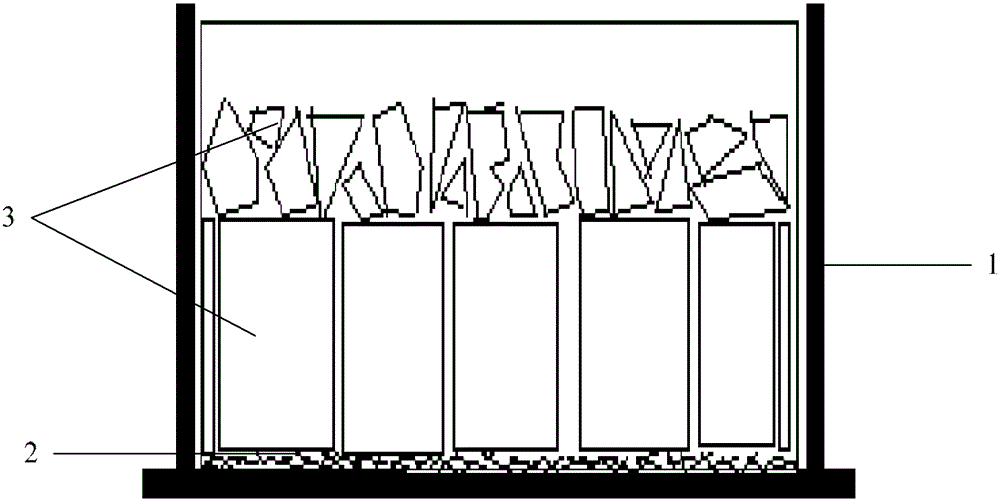
[0047] Take a quartz crucible, spray a layer of silicon nitride coating on the inner wall of the crucible, and lay a layer of polysilicon scraps with a size of 1-5 cm and a thickness of 1 cm on the bottom of the crucible. After laying the bedding, fill various block silicon materials on the polysilicon scraps until all of them are filled. figure 1 It is a schematic diagram of this embodiment after charging, wherein 1 is a crucible, 2 is polysilicon scrap, and 3 is silicon material.
[0048] Put the above-mentioned crucible with silicon material into the ingot casting furnace, start the ingot casting process, vacuumize, and then heat to the melting point of silicon to slowly melt the silicon material. In the melting stage, use a quartz rod to detect the position of the solid-liquid interface formed by the silicon melt and unmelted silicon material. In the early stage of the melting stage, the detectio...
Embodiment 2
[0056] A method for preparing a polycrystalline silicon ingot, comprising:
[0057] Take a quartz crucible, and spray a layer of silicon nitride coating on the inner wall of the crucible. First lay a layer of polysilicon block with a thickness of 1 cm on the bottom of the crucible, and then lay a layer of polycrystalline scrap with a size of 1 to 5 cm and a thickness of 2 cm on it. After laying the bedding, fill various block silicon materials on the polycrystalline crumbs until all of them are filled.
[0058] Put the above-mentioned crucible with silicon material into the ingot casting furnace, start the ingot casting process, vacuumize, and then heat to the melting point of silicon to slowly melt the silicon material. In the melting stage, use a quartz rod to detect the position of the solid-liquid interface formed by the silicon melt and unmelted silicon material. In the early stage of the melting stage, the detection is carried out every 1h, and in the late stage of the ...
Embodiment 3
[0065] A method for preparing a polycrystalline silicon ingot, comprising:
[0066] Take a quartz crucible, and spray a layer of silicon nitride coating on the inner wall of the crucible. First lay a layer of graphite plate with a thickness of 1cm on the bottom of the crucible. The graphite material is three-high graphite, and then lay a layer of polycrystalline scrap with a size of 1-5cm and a thickness of 0.5cm on it. After laying the bedding, fill various block silicon materials on the polycrystalline crumbs until all of them are filled.
[0067] Put the above-mentioned crucible with silicon material into the ingot casting furnace, start the ingot casting process, vacuumize, and then heat to the melting point of silicon to slowly melt the silicon material. In the melting stage, use a quartz rod to detect the position of the solid-liquid interface formed by the silicon melt and unmelted silicon material. In the early stage of the melting stage, the detection is carried out ...
PUM
| Property | Measurement | Unit |
|---|---|---|
| thickness | aaaaa | aaaaa |
| thickness | aaaaa | aaaaa |
| size | aaaaa | aaaaa |
Abstract
Description
Claims
Application Information


