
Ferrite circuit board

a circuit board and ferrite technology, applied in the direction of printed circuit aspects, transformer/inductance coil/winding/connection, transformer/inductance details, etc., can solve the problems of reducing the structural stability allowing a limited amount of current, and affecting the connection strength between the wires and the substrate, etc., to achieve abundant functionality, improve the connection strength between the wire and the substrate, and increase the cross-sectional area

Inactive Publication Date: 2015-03-05
IBIS INNOTECH
View PDF5 Cites 0 Cited by
  • Summary
  • Abstract
  • Description
  • Claims
  • Application Information

AI Technical Summary

Benefits of technology

This patent improves the connection strength between a wire and a substrate by embedding the wire in a groove on the substrate. The groove has a rough inner wall and is designed to accommodate the wire, which allows for a larger amount of current to flow through it. The groove can also be shaped to fit the wire, making it suitable for use as an inductor. These improvements come with increased functionality for the circuit board.

Problems solved by technology

However, because the wires of the conventional circuit board protrude from the surface of the substrate, the wires may be easily separated from the substrate in the subsequent manufacturing process of the circuit board.
Besides, when the part of the seed layer is etched, the seed layer located between the wires and the substrate is liable to be separated from the substrate due to over-etching.
In addition, with the tendency of miniaturized-sized electronic elements, the wire of the circuit board is required to be made thinner, thereby reducing the contact area between the wires and the substrate, which in turn resulting in decrease of the structural stability between the wires and the substrate.
Further, because the width and the thickness of the wire are respectively limited by usage requirement and sputtering process, the cross-sectional area of the wire is limited, such that it can only allow a limited amount of current to flow therethrough.

Method used


Image

  • Ferrite circuit board
  • Ferrite circuit board
  • Ferrite circuit board

Examples


Embodiment Construction

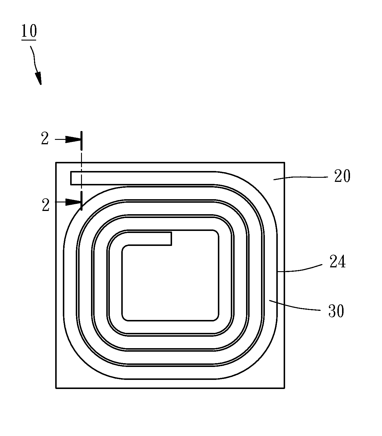
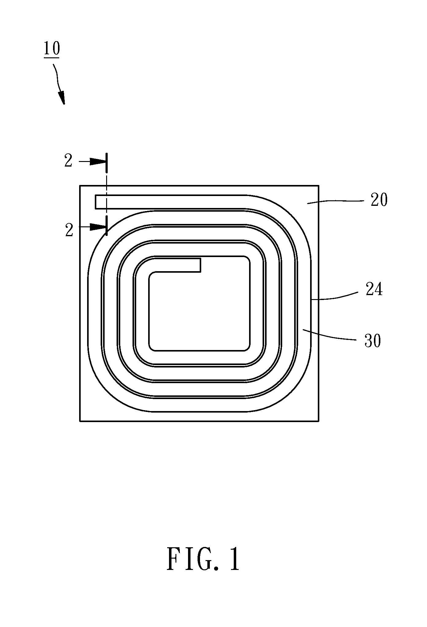
[0013]The structure and effect of the present invention will become more fully understood from the detailed description given herein below and the accompanying drawings. Referring to FIG. 1, a ferrite circuit board 10 according to a preferred embodiment of the present invention comprises a substrate 20 and a wire 30.

[0014]The substrate 20 is formed by sintering ferrite powder and the examples of ferrite powder may be Mn—Zn ferrite powder, Ni—Zn ferrite powder, Ni—Cu—Zn ferrite powder, Mn—Mg—Zn ferrite powder, Mn—Mg—Al ferrite powder, Mn—Cu—Zn ferrite powder, Co-ferrite powder, or the combination thereof. In another embodiment, the substrate 20 may be made of ferrite formed by another process.

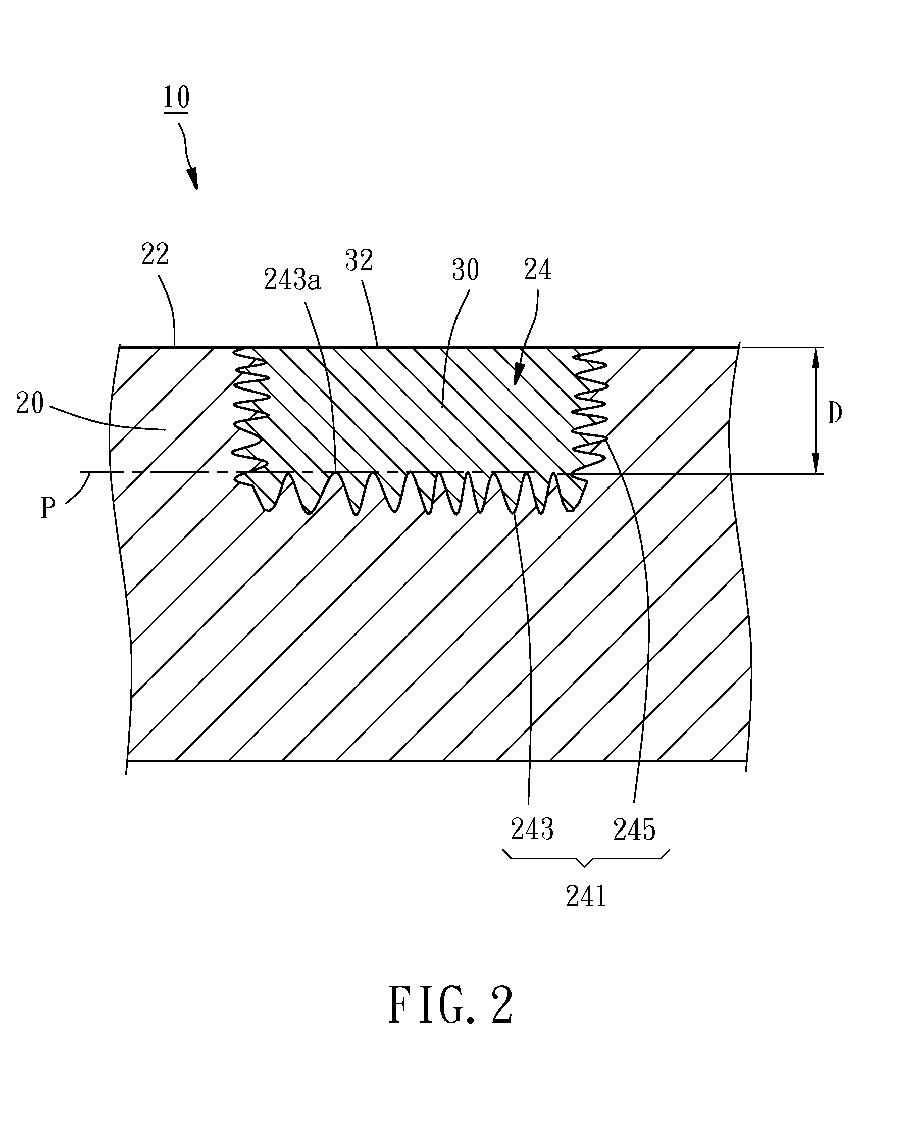
[0015]As shown in FIG. 2, the substrate 20 has a surface 22 and an elongated groove 24 recessed from the surface 22. The elongated groove 24 includes an inner wall 241 having a bottom surface 243 and two side surfaces 245. The bottom surface 243 and the side surfaces 245 of the inner wall 241 ar...


PUM

PropertyMeasurementUnit
Raaaaaaaaaaa
Raaaaaaaaaaa
Raaaaaaaaaaa

Abstract

A ferrite circuit board includes a substrate and a wire. The substrate is made of ferrite and provided with a surface and an elongated groove recessed from the surface. The elongated groove has an inner wall having a roughness Ra ranging from 0.1 μm to 20 μm. The wire is embedded in the elongated groove of the substrate, such that the wire is not easily separated from the substrate. The ferrite circuit board can be used as an inductor to provide abundant functionality.

Description

CROSS-REFERENCE TO RELATED APPLICATION[0001]This application claims priority from Taiwan Patent Application No. 10221672.3 field on Sep. 5, 2013, the entire content of which is incorporated herein by reference.BACKGROUND OF THE INVENTION[0002]1. Field of the Invention[0003]The present invention relates generally to circuit boards and more particularly, to a ferrite circuit board with firm structure and can be used as an inductor.[0004]2. Description of the Related Art[0005]A conventional circuit board primarily comprises an insulated substrate and a plurality of wires attached on a surface of the substrate. In the manufacturing process of the circuit board, a conductive material such as nickel-chromium alloy is first coated on the surface of the substrate by sputtering to serve as a seed layer thereon. Subsequently, a photolithography process is performed and a metal material such as copper is electroplated on the seed layer to form the wires. Thereafter, part of the seed layer that...

Claims


Application Information

Patent Timeline
Patent Type & Authority Applications(United States)
IPC IPC(8): H01F27/28
CPCH01F27/2804H01L33/62H01L2924/0002H01L23/15H01L23/49838H01L2924/00H01L33/486H05K1/0306H05K2201/0175
Inventor LAI, WEI-JENHUANG, CHIH-KUNG
Owner IBIS INNOTECH
Learn More