Bonding member

a technology of bonding member and bonding plate, which is applied in the direction of superimposed coating process, soldering apparatus, manufacturing tools, etc., can solve the problem of re-melted solder

Inactive Publication Date: 2015-03-12
MURATA MFG CO LTD
View PDF2 Cites 8 Cited by
  • Summary
  • Abstract
  • Description
  • Claims
  • Application Information

AI Technical Summary

Problems solved by technology

However, the melting point of the solder after connecting the pad for external connection and the electronic component does not change very much from before the connection, and there is a problem, for example, that when the solder is passed through a reflow furnace again for mounting additional electronic component, the solder is re-melted to shift the bonded position of the electronic component connected once.

Method used


Image

  • Bonding member
  • Bonding member
  • Bonding member

Examples


experimental example

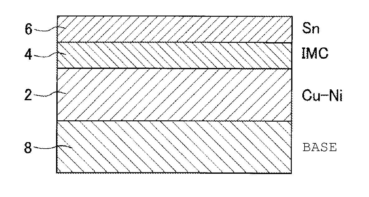
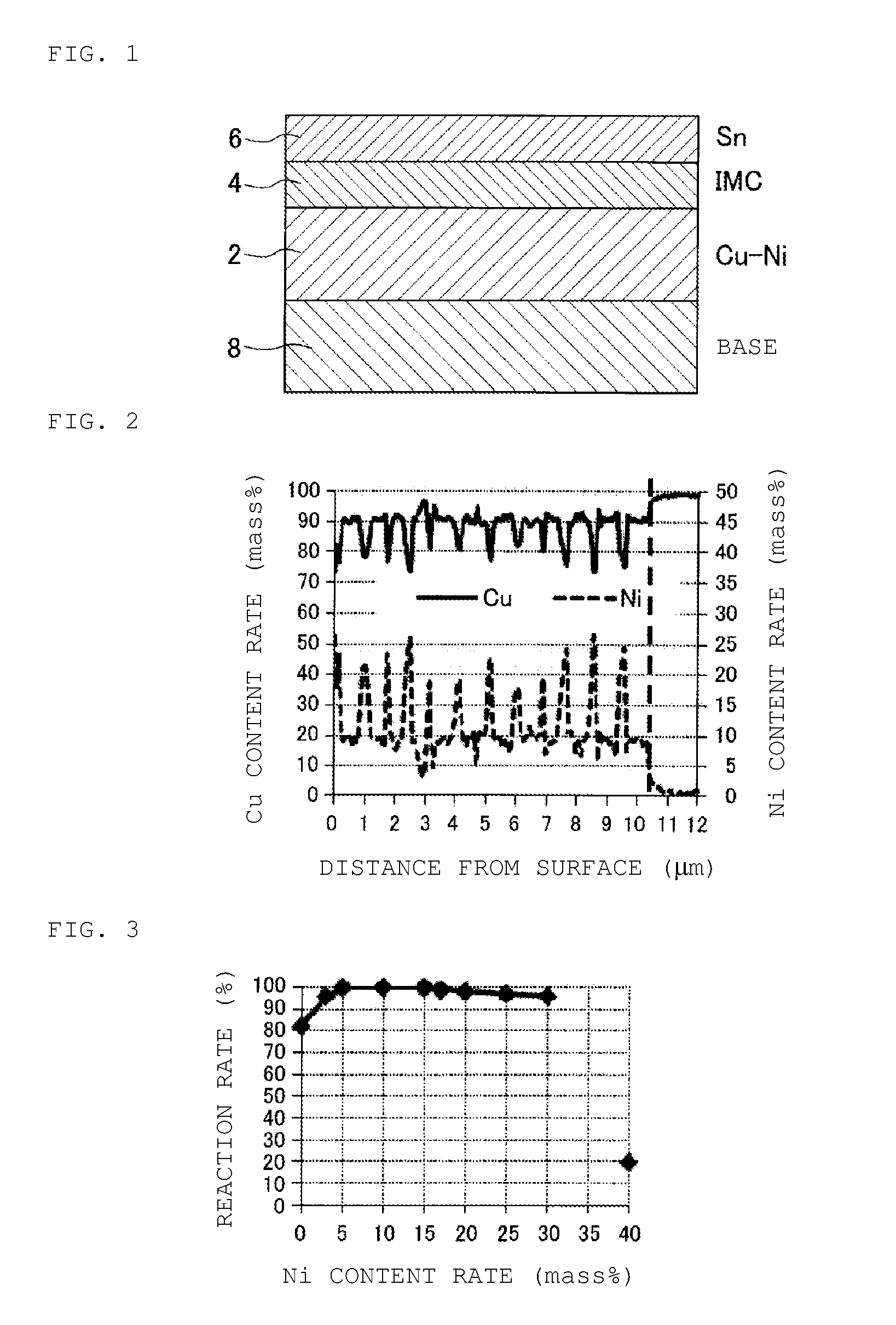
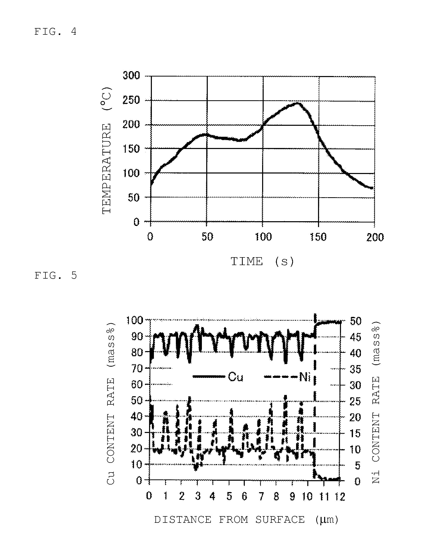
[0042]In the experimental example, as the following Example 1, Example 2, Comparative Example 1, Comparative Example 2, Comparative Example 3, and Comparative Example 4, six types of samples including Cu—Ni alloy plating films formed under different conditions were created by applying Cu—Ni alloy electrolytic plating to the surface of a base to form a Cu—Ni alloy plating film containing a Cu—Ni alloy as its main constituent, and then applying Sn electrolytic plating to form a Sn plating layer, and the samples were evaluated.

[0043]A glass epoxy substrate (wiring substrate) with a number of Cu electrode patterns formed on the surface of the substrate was used for the base. More specifically, with the Cu electrode patterns on the glass epoxy substrate as the base, the surfaces of the Cu electrode patterns were subjected to electrolytic plating. The Cu electrode patterns each have a rectangle shape of 0.8 mm in the X direction (transverse direction) and 1.5 mm in the Y direction (longit...

example 1

[0044]In the Cu—Ni alloy electrolytic plating for the sample according to Example 1, as a plating solution, a mixed aqueous solution of 0.03 mol / L of nickel sulfate hexahydrate, 0.06 mol / L of copper sulfate pentahydrate, and 0.15 mol / L of sodium gluconate was used into which an appropriate amount of a film conditioner was put. The pH of the plating solution was 4.5, and the temperature of the plating solution was 40° C. Then, the electrolytic plating current set at 80 A / m2 for 2 minutes and set at 150 A / m2 for 5 minutes was regarded as one cycle, and 12 cycles were implemented. As a result, a Cu—Ni alloy plating film of 10 μm in thickness, containing a Cu—Ni alloy as its main constituent was formed on the surface of the base (Cu electrode pattern).

example 2

[0045]In the Cu—Ni alloy electrolytic plating for the sample according to Example 2, as a plating solution, a mixed aqueous solution of 0.03 mol / L of nickel sulfate hexahydrate and 0.2 mol / L of copper sulfate pentahydrate was used into which appropriate amounts of a complexing agent and a film conditioner were put. The pH of the plating solution was 5.0, and the temperature of the plating solution was 50° C. Then, the electrolytic plating current set at 80 A / m2 for 1 minute and set at 300 A / m2 for 2 minutes was regarded as one cycle, and 12 cycles were implemented. As a result, a Cu—Ni alloy plating film of 10 μm in thickness, containing a Cu—Ni alloy as its main constituent was formed on the surface of the base (Cu electrode pattern).


PUM

PropertyMeasurementUnit
mass ratioaaaaaaaaaa

Abstract

A bonding member that includes a plating film containing a Cu—Ni alloy as its main constituent. In this plating film, the Cu mass ratio Cu/(Cu+Ni) is increased and decreased between 0.7 and 0.97 in the film thickness direction. In addition, the amplitude between the increase and decrease in the Cu mass ratio is larger than 0.1. Therefore, when the plating film containing the Cu—Ni alloy as its main constituent and Sn-based solder material or the like are joined by soldering, an intermetallic compound layer with a high melting point is formed. In addition, the plating film has a layer with a slow reaction rate, and thus can slow the reaction rate of alloying reaction between the Cu—Ni alloy and a Sn-based metal.

Description

CROSS REFERENCE TO RELATED APPLICATIONS[0001]The present application is a continuation of International application No. PCT / JP2013 / 065972, filed Jun. 10, 2013, which claims priority to Japanese Patent Application No. 2012-138076, filed Jun. 19, 2012, the entire contents of each of which are incorporated herein by reference.FIELD OF THE INVENTION[0002]The present invention relates to a bonding member, for example, for bonding between an attachment electrode and an electronic component which are formed on a wiring substrate.BACKGROUND OF THE INVENTION[0003]The wiring substrate described in Patent Document 1 has a pad for external connection, which includes a surface plating layer. The surface plating layer is formed from a combination of Ni and Au, a combination of Ni, Pd, and Au, or a combination of Sn or Sn with Ag. In addition, the pad for external connection is formed from Cu or a Cu alloy.[0004]Patent Document 1: Japanese Patent Application Laid-Open No. 2008-300507SUMMARY OF THE...

Claims


Application Information

Patent Timeline
Patent Type & Authority Applications(United States)
IPC IPC(8): H05K3/40B23K35/26B23K35/02C25D3/56C25D5/16
CPCH05K3/40C25D3/56H05K2203/04B23K35/0238B23K35/262C25D5/16B23K1/20B23K1/0016B23K1/008H05K3/225H05K3/244H05K3/341H05K2201/0338B23K35/226C23C28/02C23C28/021C25D3/58C25D5/10C25D5/18C25D5/505C25D21/12C25D21/14B23K35/0222B23K35/0233B23K2101/42Y10T428/12458
Inventor SUNAGA, TOMOHIROMEGUMI, DAISUKETAKANO, YOSHIHIKOTAKAOKA, HIDEKIYO
Owner MURATA MFG CO LTD
Why Eureka
Try Eureka