Nonvolatile semiconductor storage device and control method thereof
a nonvolatile semiconductor and storage device technology, applied in static storage, digital storage, instruments, etc., can solve the problems of double page buffer circuits and increase in chip size, and achieve the effect of improving the read speed of memory cells
- Summary
- Abstract
- Description
- Claims
- Application Information
AI Technical Summary
Benefits of technology
Problems solved by technology
Method used
Image

Examples
first embodiment
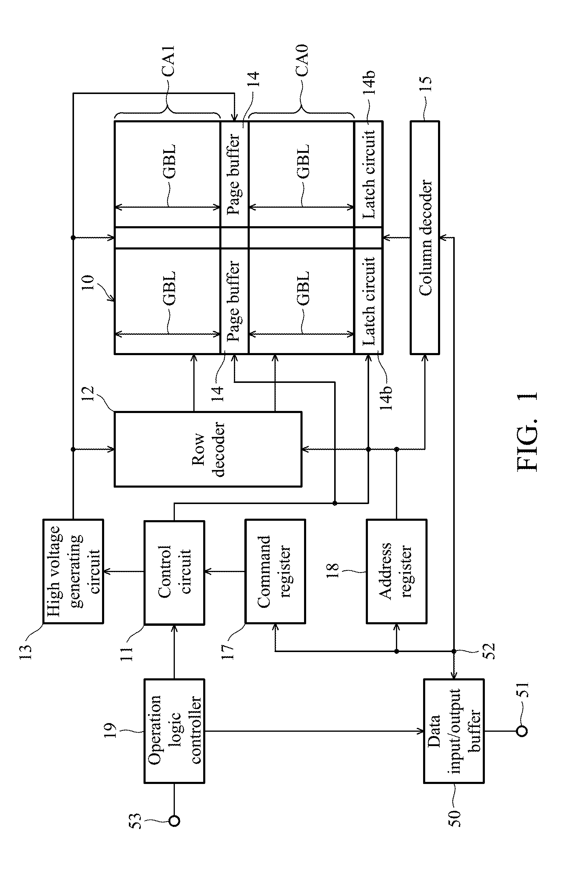
[0066]FIG. 2 is a circuit diagram illustrating a memory cell array 10 and the peripheral circuits of the NAND-type flash EEPROM according to a first embodiment of the invention.
[0067]In FIG. 2, the cell array CA0 comprises a plurality of block size cell arrays BSCA0, and each of the block size cell arrays BSCA0 comprises a pair of global bit lines GBLe, GBLo connected to plural memory cells respectively. By this, a plurality of electrical-rewritable and nonvolatile memory cells MC0-MC15 with stacked-gate structure connected in series are provided in the pair of global bit lines GBLe, GBLo. The global bit line switch circuit 21, 22 are provided at both sides of the ends of the pair of global bit lines GBLe, GBLo, and select one of the global bit lines GBLe and GBLo to connect with the corresponding circuit. In addition, the cell array CA1 comprises a plurality of block size cell arrays BSCA1, and each of the block size cell arrays BSCA1 comprises a pair of global bit lines GBLe, GBLo...
second embodiment
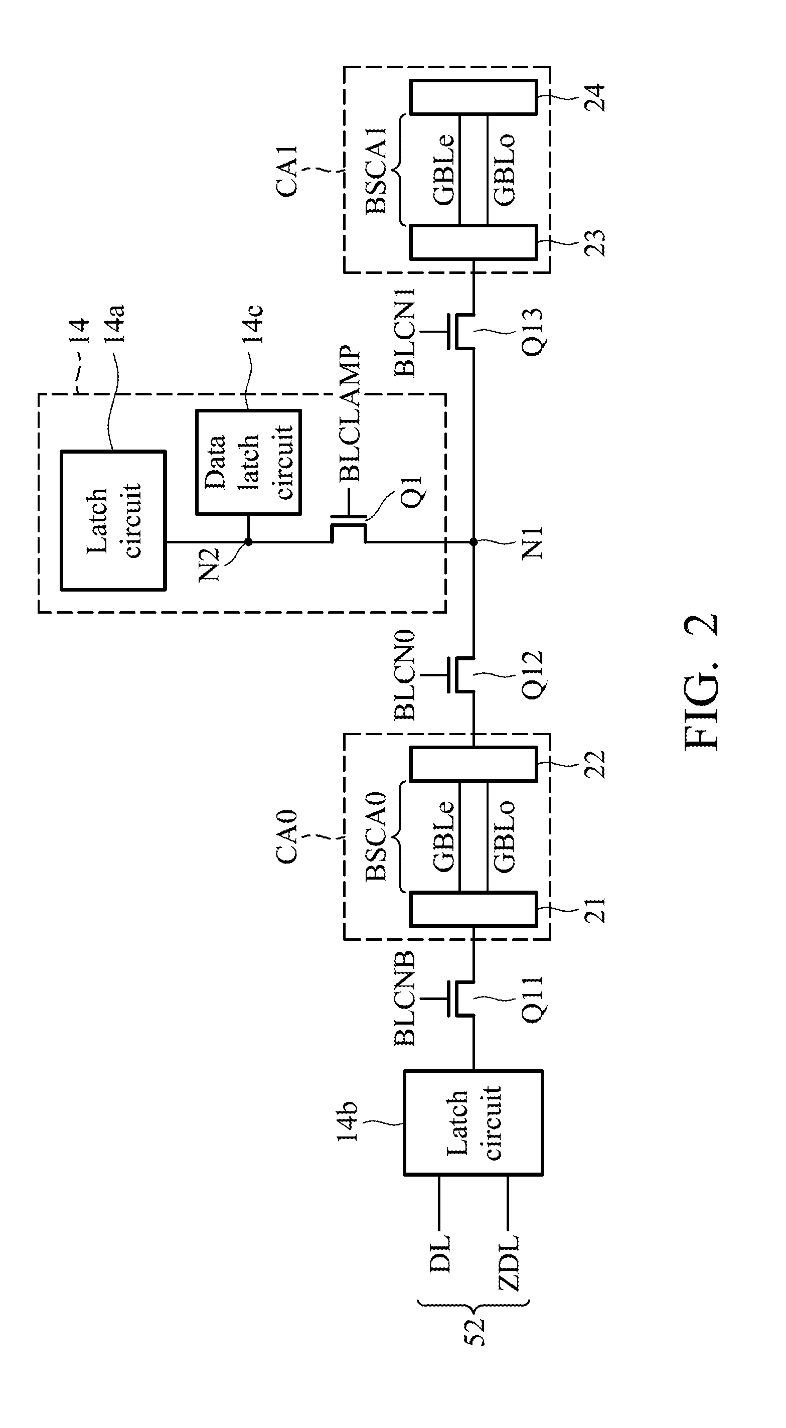
[0078]FIG. 3A is a circuit diagram illustrating a memory cell array 10 and the peripheral circuits of the NAND-type flash EEPROM according to a second embodiment of the invention. Although the data to the page buffer circuit 14 or the data from the page buffer circuit 14 is transmitted through the global bit line GBLo or GBLe of the cell array CA0 in the circuit of FIG. 2, there are the following differences between the circuit in FIG. 2 and the circuit in FIG. 3A: (1) using a device with multiple layers, the data bit line DBL connecting node N1 and the latch circuit 14b are installed in a higher layer than the memory cell. In the embodiment, the two layers can be connected via the via-conductor. The differences are described in the following paragraphs.
[0079]In FIG. 3A, the latch circuit 14b is connected to the node N1 through the MOS transistor Q14 controlled by the control signal DSW0, the data bit line DBL and the MOS transistor Q15 controlled by the control signal DSW1. Because...
third embodiment
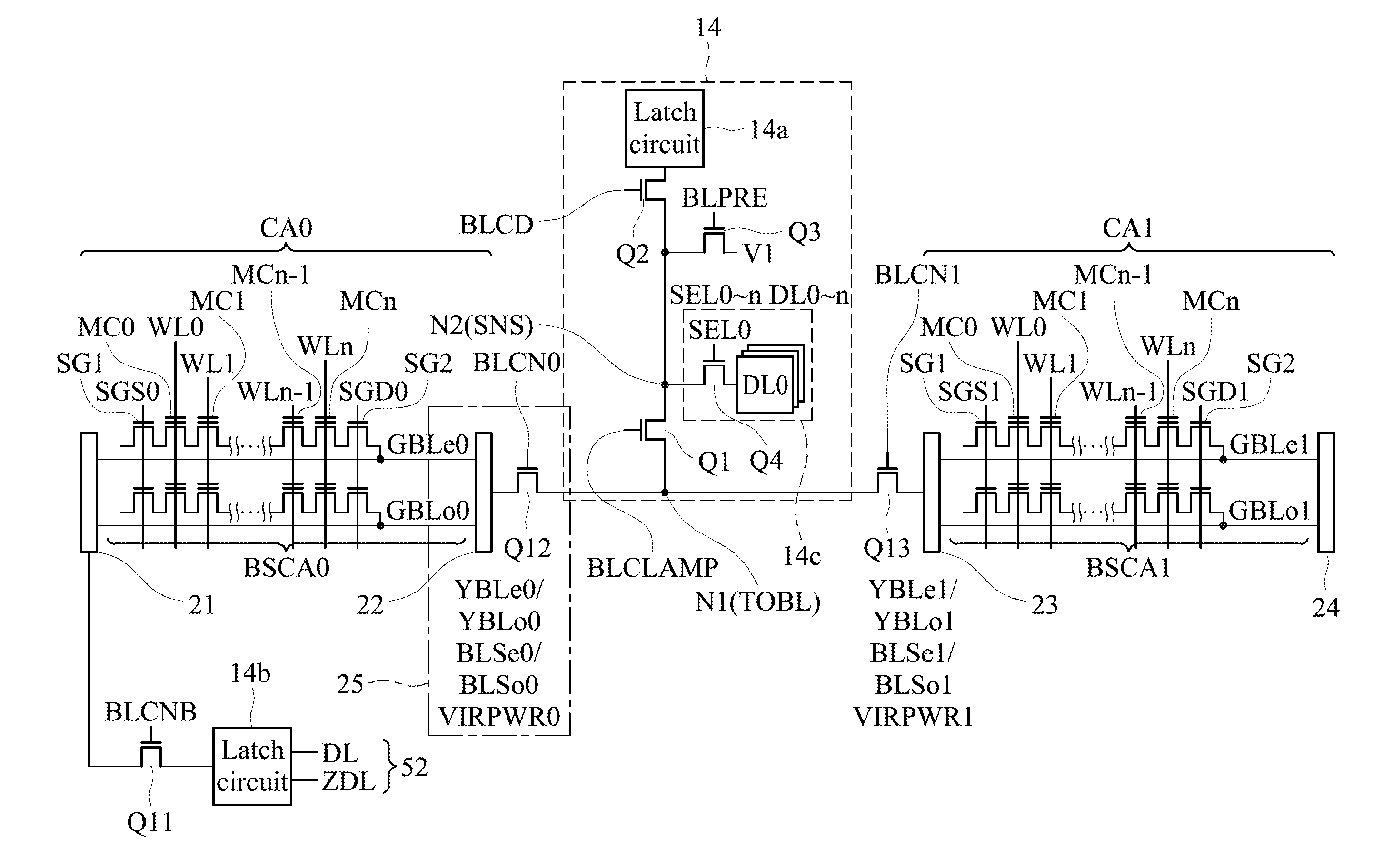
[0086]FIG. 4A is a circuit diagram illustrating a memory cell array 10 and the peripheral circuits of the NAND-type flash EEPROM according to a third embodiment of the invention, FIG. 4B is a circuit diagram illustrating the detailed composition of the global bit line switch circuit part 25 in FIG. 4A. In the embodiment, the third embodiment is the specific example concretely illustrating a circuit of the first embodiment.
[0087]There are the following differences between the circuit in FIG. 2A and the circuit in FIG. 4A. (1) The block size cell arrays BSCA0 and BSCA1 comprise selection transistors SG1 and SG2, and a NAND cell unit formed by a plurality (n) of electrical-rewritable and nonvolatile memory cells MC0-MCn with stacked-gate structure connected in series is connected to the pair of global bit lines GBLe, GBLo. In the embodiment, the control gates of each memory cell MC0-MCn forming a line in the row direction are commonly connected to word lines WL0-WLn respectively, and t...
PUM
 Abstract
Description
Claims
Application Information
 - Generate Ideas
- Intellectual Property
- Life Sciences
- Materials
- Tech Scout
- Unparalleled Data Quality
- Higher Quality Content
- 60% Fewer Hallucinations
Browse by: Latest US Patents, China's latest patents, Technical Efficacy Thesaurus, Application Domain, Technology Topic, Popular Technical Reports.
© 2025 PatSnap. All rights reserved.Legal|Privacy policy|Modern Slavery Act Transparency Statement|Sitemap|About US| Contact US: help@patsnap.com